Let's Design and Build a (mostly) Digital Theremin!

Posted: 3/18/2025 9:28:31 AM
dewster

From: Northern NJ, USA

Joined: 2/17/2012

Thank you bisem!  I think I was over articulating the volume a bit, and the pitch could have used more glissando / portamento.  Would have preferred piano accompaniment as the guitar chording (as played by this rather simple player) is rather simplified.  I know I'm always moaning about this, but adding even one instrument to the mix makes a recording like this take days instead of sometimes just minutes a cappella.

There's something about the timing in this hymn that made it difficult too, 3/4 time and starting on the up beat kept throwing me off for some reason.

Posted: 4/2/2025 9:56:19 AM
Buggins

From: Porto, Portugal

Joined: 3/16/2017

Posted yet another candidate for the new D-Lev AFE - in Wallin Oscillator thread

Posted: 4/5/2025 1:01:18 PM
dewster

From: Northern NJ, USA

Joined: 2/17/2012

Vadim, thank you for that!  I replaced the drive CMOS inverters with my 4 transistor buffer, and simplified the current mirror:

Haven't benched it yet.  The sim draws ~15mA and seems to tolerate a certain amount of drive capacitance (Ccoax), which might allow co-location on the main PCB.  The main thing that scares me at this point is the delay introduced by the current mirror and C4, which might be rather temperature dependent?  I'm not sure emitter degeneration resistors R3 & R4 are necessary, but I worry about thermal runaway here.  Link to the LTspice file: https://d-lev.com/research/afe_ve_2025-04-04.asc.zip

Posted: 4/5/2025 8:38:10 PM
Buggins

From: Porto, Portugal

Joined: 3/16/2017

[dewster] The main thing that scares me at this point is the delay introduced by the current mirror and C4, which might be rather temperature dependent?  I'm not sure emitter degeneration resistors R3 & R4 are necessary, but I worry about thermal runaway here.


Definitely, there should be big enough latency introduced by current mirror running in this mode.
Current mirror may give you almost zero (<1ns) latency when integrated voltage does not exceed the limits switching them to into saturation.
Just increase C4 to keep integrator output within 0.5V from power rails. One more thing missing in your current sensor is a biasing for C4.
Now it's biased due to the limits by rails. Once amplitude go beyond the limits, sense signal will turn into sine touching positive or negative rail, with distortion close the rail.
Putting high nominal resistors to bias around VCC/2 (e.g. 47K or 100K) should give better result, pure sine wave centered close to VCC/2.
Another concern can be simplification of current mirrors - 2-BJT mirror will give bigger output range but probably bigger delay or less linearity (not sure).
But it will make it harder to convert to square wave. Fast comparator (e.g. adcmp600) might do such conversion (see v2, v3, v4 versions of AFE on github).
Another issue with this type of current sensing (integration) that with the same current, lower frequency you will get higher voltage swing on output, and higher frequency will give lower swing.
Using of comparator and choosing proper C4 value keep the current sensing sine output below bounds in frequency and current range could help.

I'm not sure about R3 and R4, but I have concern regarding R1, R2. Doesn't it makes sense to replace them with current sources? (+4 BJTs)

Is your goal to design BJT + invertor only AFE?

Posted: 4/9/2025 6:51:23 PM
dewster

From: Northern NJ, USA

Joined: 2/17/2012

"... but I have concern regarding R1, R2. Doesn't it makes sense to replace them with current sources? (+4 BJTs)"  - Buggins

I tried that (in simulation) and it restricts the drive swing, and hence the max Vpp at the antenna.

"Is your goal to design BJT + invertor only AFE?"

Good question! :-)  The ultimate goal is the best possible AFE regardless of anything else, but there are various attractive features associated with various approaches that are sometimes difficult to ignore.

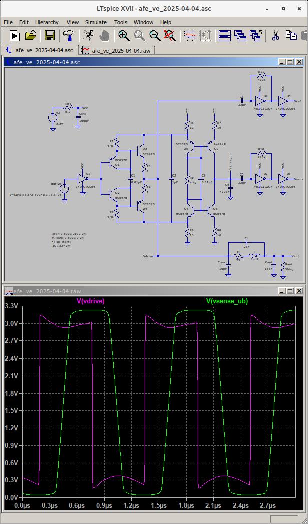
Here's the circuit I'm currently playing with:

R1 and R2 now go to directly to +3V & ground, they don't draw much current so connecting them via R5 & R6 won't influence the current sensing much at all.  As you suggested, I added R10 & R11 to help center the integrated output, which was otherwise moving around a lot when there was no clipping going on.

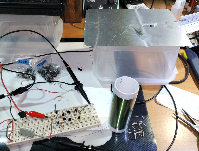
Here it is on the bench, running open-loop, driven by my function generator:

And here it is running closed-loop, driven by my lab D-Lev pitch side:

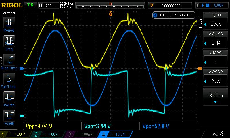
Light blue trace is the square wave drive at the coil, yellow trace is the integrator output, dark blue trace is my medium voltage probe connected to the antenna plate.  Phase looks really good, and the > 500 Vpp looks great (Thereminis everywhere are going to cry)!  It doesn't seem to drift terribly.  This is directly connecting the transistors to the FPGA with no CMOS to square things up.  The noise looks to be 5x or 10x worse than the C divider approach, with some random tearing, but it's on my noisy bench, no CMOS buffering, etc. so not exactly apples to apples.

Thoughts:
1. The expanded drive voltage swing really boosts the antenna voltage.  The drive buffer at least seems like a keeper.
2. The integrator gain can be adjusted via R9, so this could perhaps be a "tuning" potentiometer, like 10k in series with 1k.
3. The integrator output and antenna voltage phases track well, though there is a bit of tracking difference when the integrator is clipping, which was expected, but it's interesting to see it happening dynamically, and doesn't seem to be a huge deal.
4. The integrator output is obviously nowhere near as smooth as the antenna voltage, which for all practical purposes is a pure sine wave.  Lowering the integrator gain would make it more sine-like, but that would allow it to move around somewhat too.  The spikes riding on it aren't occurring near the zero crossing, which is good.
5. While it's nice that we're sensing current at the drive side of the coil, rather than voltage at the exposed high impedance side, we're having to cancel out the drive current with an integrating mirror.  I think this unavoidably introduces more noise into the sensing than the old C divider way.
6. The C divider approach takes the antenna voltage, divides it down by about 100:1, and then jacks the edges back up via CMOS inverter gain.  While the reduction and subsequent gain-up might seem like an SNR killer, the voltage is a very pure high voltage sine wave, and any interference gets severely attenuated along with it.  The main downside here is the divider needs to be tuned in order to stay within the linear region, not too big and not too small, and the tuning itself is awkward.
7. Making the C divider more like my medium voltage probe and positioning it at the center axis of the coil (where the electric field is minimal) is looking better and better.  The AFE would then be mounted at the "cold" low impedance drive end of the coil.
8. These experiments make me want to implement a watchdog of some sort on the phase detection to prevent harmonic locking.

You must be logged in to post a reply. Please log in or register for a new account.