


Fred, that is generous of you. Having a design to take to a builder would be great! Thank you.
Gordon. :-)

From: Eastleigh, Hampshire, U.K. ................................... Fred Mundell. ................................... Electronics Engineer. (Primarily Analogue) .. CV Synths 1974-1980 .. Theremin developer 2007 to present .. soon to be Developing / Trading as WaveCrafter.com . ...................................
Joined: 12/7/2007
Hi Gordon,
As you are on holiday, I will put this design together slowly as a complete "technical file" and include any relevant links that could be useful (or essential) for whoever builds this thing - Even if this design is not used, it should help convey some ideas.
It would be great if you could convey to any interested party that I am available to take on design work (particularly when paid ;-) for any electronic stuff, particularly audio and analogue - anything really except DSP ;-)
I will add to this posting unless it becomes too massive, and will also put a .pdf of the whole lot on Element-14 when completed <Link to complete design> <- Will be inserted when i'm done.
------------------------------------
Proposed possible circuitry for FSR based pedal – Part 1
© Fred Mundell Aug 2014
Permission is granted for use of this material for non-commercial use.
Copies of these notes and designs may be made / distributed only if this header is retained and the contents are not edited and no part is deleted.
----------------------------------
Force sensing resistor data:
http://www.rapidonline.com/pdf/78-4000.pdf
Bigger (0.5") FSR (probably better)
Big FSR @£7.22 probably best From Rapid
I have some small FSR's somewhere - Bigger ones tend to be a bit pricey. Best configuration would probably be to fix the sensor to a pad so it operates with a force (?)* above 100g in its more linear region perhaps >50g to activate, and 500g for maximum, giving resistance >20k when "off" and from about 20k to 5k from min to max.. I will design the electronics on this basis, but the range can be changed by changing a few resistor values.
The design will be split into sections:
1.) Force sensor amplifier
2.) Envelope generator (simple AR - two versions)
3.) Switchable inverting / non-inverting buffer (to facilitate normal or inverted envelope)
4.) VCA (using both halves of LM13700 in series to improve law)
5.) Regulator.
The Force sensor amplifier will include bias and gain controls which can be presets or replaced with user control - this will allow 'leakage' and 'depth' of effect to be adjusted. Likewise the envelope generator attack and release will be adjusted by presets which can be replaced by user controls. One single pole switch will set either 'normal' or 'inverted' operation.
'Normal' operation = Audio is output when pedal is pressed.
'inverted' = Audio is attenuated when pedal is pressed.
I know your wish to keep it as simple as possible, and will only include what I deem to be the absolute minimum required to achieve the desired objectives in a reliable way - I am looking at one dual op-amp, one LM13700, one regulator, a couple of diodes, perhaps 15 resistors, perhaps 8 small capacitors, and 5 preset resistors/potentiometers some of which could be user adjustable potentiometers (controls), switch / connectors ,FSR pad and mechanical bits will need to be added by the builder.
*Not sure about the word "force" - to me there is some ambiguity here as force should be in newtons not grams? - perhaps this is because the areas of these sensors varies, so grams distributed over the area equates to force - as in, a small sensor with 100 grams on it gives the same resistance as a large sensor with 100 grams on it, but the small sensor would be under greater force per unit area than the large sensor...
-----------------------------------------------------
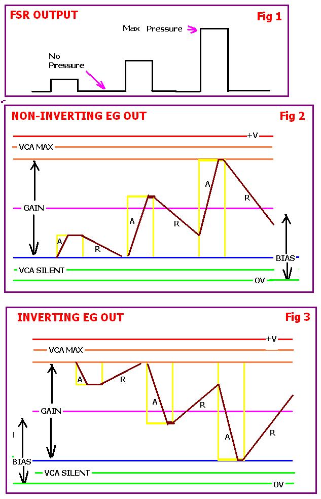
Proposed basic sensor / EG operation:
Pressure on pedal converts to changing resistance on FSR, this is converted to changing voltage as shown. Gain and biasing of the amplified FSR voltage is adjustable, and the voltage from this amplified / shifted FSR voltage drives the EG (Envelope Generator).
If the EG attack and release are short, the pedal will act in a linear mode, whereby pressure on the pad will directly control the VCA - Usual operation however is likely to be tapping of the pedal and driving the EG, which usually has fast attack and slower release.
By adjusting the gain and bias it is possible in "normal" mode to allow some audio to pass through the VCA even when the pedal is not pressed, or to adjust the bias so that audio is only output when it is pressed.
In inverting mode, audio is output when the pedal is not pressed, and attenuated when it is pressed - The inverted mode simply flips the control waveform about the mid voltage, and if "correctly" set, neither gain nor bias will need adjusting to change modes - Bias will have far more influence on "normal" mode.
=======================================================
Please note: "Bias" in the above description has now been called "OFFSET" in the following, and "bias" in the following is just a one-time adjustment unrelated to the above use of the word.
FSR AMPLIFIER:
This amplifier is awkward only because the FSR resistance changes will be subject to the mechanical aspects of the pedal, which at this time are unknown. I have designed it so that by minimal changes (resistor values) hopefully it will cater for any realistic construction.
Two user controls are provided (these could be presets), one for gain, the other for offset - I used two opamps in this design (one dual op-amp) to make these controls entirely independent of each other (a simpler scheme could be implemented, but these controls would then interact).
Full description is coming soon, for now though, the schematics:
PLEASE NOTE! - THIS HAS NOT BEEN BUILT, HAS ONLY BEEN SIMULATED! - Its simple enough that it really should work as per simulation, but its never wise to fully trust that real circuits will behave the way the simulator says they will! ALWAYS BREADBOARD BEFORE COMMITTING TOO MUCH TIME OR MONEY!
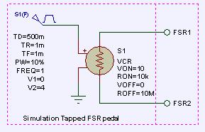
1.) Simulation model for tapped FSR - the voltage from the pulse generator modulates the virtual resistance, so I was able to test for different forces. This circuit is not built - its just for simulation.
FIG 4:
2.) The FSR Amplifier:
FIG 5:
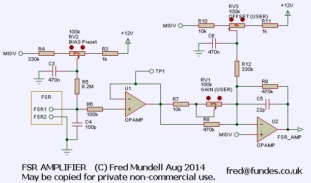
FIG 6:
3.) Circuit description briefly:
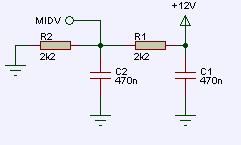
Supply voltage (12V but could be 9V) halved by R1 / R2 to give MIDV.
FSR when not pressed gives about 10M resistance, and lower when pressed - RV2 (bias preset) is adjusted so that when FSR is not pressed, the output voltage on TP1 is the same as that on MIDV (this is set first, and not adjusted again). When this is done, the output (TP1) will drop from MIDV towards -V every time (and while) the FSR is tapped or force is applied to it, the voltage will follow the pressure applied to the FSR continuously.
R7 sets the maximum gain (amplification) of the FSR signal, decreasing its value increases gain - best not to reduce this value below about 2k2... This is a huge gain, this resistor will probably need to be greatly increased (perhaps even to 47k) if the pedal construction is sensitive.
R7 in combination with RV1 gives user control of gain - R9 in fact determines gain in combination with these resistors, but I choose to leave R9 fixed unless one really needs to change it (increasing it increases gain) because if it is changed, R12 will also need to be changed.
R8 is just me being pedantic and providing a path for further trimming - also keeps connection if gain pot goes faulty.
R12 facilitates input of the offset voltage. RV3 is a user adjustable offset control.
[construction note: - I would swap RV1 and R7 so that any user control was not connected directly to the op-amp input, particularly if wired connection is used]
I have already gone one op-amp over budget.. But this means I now have one spare in the next dual op-amp ;-)
==================================
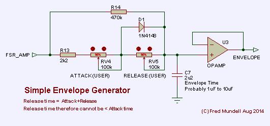
Envelope Generator:
FIG 7:
==================================
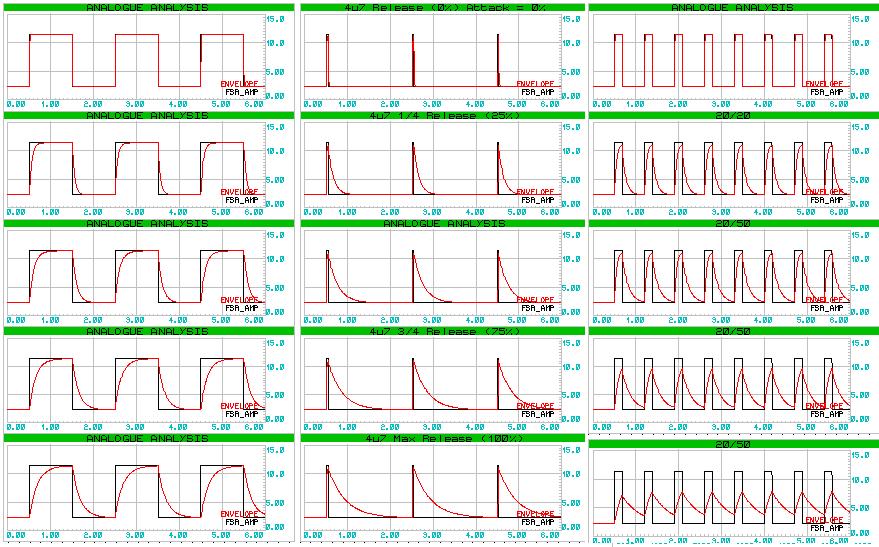
Examples of available envelopes:
Note - these simulations are with periodic pulses of constant amplitude from FSR, more complex profiles will be obtained (as per Fig 2 near top) with varying durations and FSR forces.
FIG 8:
==================================
The above envelope waveforms show the sort of curves available -Black trace is the FSR amplifier output - in reality, these will be proportional to force applied to the pad, with peak - peak amplitude being adjustable using the Gain control, and position adjustable using the Offset control - the above shows the offset at 2V, this can be shifted to 0V or up to about 6V with values given, the envelope tracks these levels.
C7 Charges and discharges via R14 (this is an optional shunting resistor for trimming and to take care of open circuit potentiometer fault) which should be at least equal to sum of RV4+RV5 in their maximum positions, Reducing R14 will reduce the span of these controls.
R13 is current limiting, and will limit the maximum attack speed. Advice: Don't change this value.
The attack path is R13 -> RV4 -> D1 -> C7
The release path is C7 -> RV5 -> RV4 -> R13
It can be seen that both the attack charge and the release discharge go through the attack potentiometer RV4, and thus release time cannot be set shorter than attack time, and if RV5 is set to 0, attack and release times will be the same (set by RV4).
I did this to simplify the circuit and eliminate the need for analogue switches and their drive circuitry - An extra diode could be added to separately steer charge and discharge paths, but this would have introduced a diode drop on the discharge path - I felt that in positive mode, this may not be a good idea as one may want to accurately set the 'silent' position for the VCA.
The circuit however is so simple that it can be crafted as required -
FIG 9:
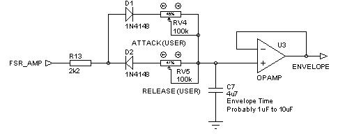
This version gives entirely independent attack and release.
==================================
I may fill in more details on the above later, but the next subjects:
3.) Switchable inverting / non-inverting buffer (to facilitate normal or inverted envelope)
4.) VCA (using both halves of LM13700 in series to improve law)
5.) Regulator.
will be on a new posting.. this one is getting too big!
Fred.
Ooh, I have some choices to make...
Um, bring able to set release shorter than attack sounds like A Good Thing - I like "reversed tape" sounds. :-) But I get the impression that "a diode drop on the discharge path" is Not A Good Thing, although I do not know why. Wild guess --> Does this increase the amount of noise in the signal?
I can see some uses for a stereo version - e.g. to cross-fade from one effects chain to another - but I think this would have limited application for me, particularly as I anticipate the pedal having a permanent place in my effects chain as a kill-switch. So let's not bother with that bit. :-)
From: Eastleigh, Hampshire, U.K. ................................... Fred Mundell. ................................... Electronics Engineer. (Primarily Analogue) .. CV Synths 1974-1980 .. Theremin developer 2007 to present .. soon to be Developing / Trading as WaveCrafter.com . ...................................
Joined: 12/7/2007
Hello Gordon,
If you want independent attack and release, there's no real problem.. its just me being pedantic!
Diodes Vf is affected by temperature, so the capacitor voltage (which controls the volume) will discharge to the diode Vf and then probably be a bit indeterminate / leak towards -V .. Yeh, a bit of gain noise, but probably no problem for "inverted" (dipping) mode - and the VCA can be biased to kill any signal in normal mode.. In general, minor variation in amplitude at the high volume side becomes insignificant / inaudible (due to the log hearing curve) so one concentrates more on getting the low envelope levels precise... Which is why I kept diodes out of the discharge path.
Which brings us to the VCA - If stereo isnt wanted (and I agree with you, I think its use would be limited - I only proposed it because I was thinking two VCA's on one LM13700) and separate A and R is wanted, the LM13700 is probably a poor choice. I would probably go for opto-coupled FETs (H11F1) or a dual fet VCA.. Slight modification of the drive circuits (a couple of transistors to boost the op-amp currents) so the H11F1's can be driven up to 10mA each, and it should be there..
But I cannot simulate the H11F1 - (problems accurately simulating the LM13700) - so some fiddling with values will be needed -
The builder may have their own preferred VCA anyway, and adapting / tweaking the envelope voltages to suite should be something they can manage.
I will draw up the H11F1 circuit - If you have any ideas about VCA's let me know.. The other choice is a THATS log VCA.
The issues re the EG (release diode etc) could be resolved easily with a little more circuitry - but I am trying to keep this minimal.. Its probably 40 years since I did any minimal synth circuits like this, and I wasnt so fussy then ;-) .. My usual method is to compare the drive voltage from the FSR amplifier to the voltage on the envelope capacitor, and use the output from this comparator to switch a 4053 analogue change-over to switch either the attack or release path into the circuit - but this is 2 more IC's.. and if adding them, one can easily use the spare switches and comparator to implement a full ADSR ;-)
Fred.
One slight 'worry' I have with this simple scheme for the EG, is the fact that the curves are exponential.. This (into a linear VCA) will give a snappy response on 'normal' mode,(should be fine in inverted mode) but may not be so nice if you are into slow attack in normal mode. Using a log VCA should linearize the curve, making it similar on both normal and inverted modes.. Having said this though, loads of early, and some modern synth EG's give simple RC curves as mine, and drive linear VCA's .. But perhaps I should look at redesigning the EG to be linear - will think about it.. Its easily done if I add a comparator and CMOS switches ;-)
From: Eastleigh, Hampshire, U.K. ................................... Fred Mundell. ................................... Electronics Engineer. (Primarily Analogue) .. CV Synths 1974-1980 .. Theremin developer 2007 to present .. soon to be Developing / Trading as WaveCrafter.com . ...................................
Joined: 12/7/2007
Hi Gordon,
I have revised and simplified the design, this is the basic COMPLETE design.
I will paste a link to a .pdf ASAP - but for now:
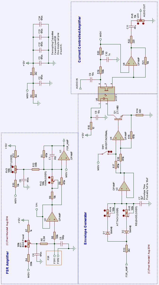
A lot of the above hasn't been simulated - (everything beyond U3 is completely untested)
U1 and U2 should be dual op-amp, U3 and U4 are a dual op-amp, U6 is an audio op-amp or dual with spare op-amp.. I am looking at using the spare either for some audio function or to buffer MIDV.
Putting provisional component values here as above may be difficult to read and its easier to change values below than to edit the image! ;-)
Ok - Should all be there now - both above and below ;-)
MidV Gen:
R2 2k2* R3 2k2* *(may change if Op-Amp used)
C2,C3, C12-C14. Ceramic decoupling capacitors - I have not done full evaluation of required values and circuits may change, but 470nF - 1uF low esr parts are usually fine (could probably reduce to 100nF but there's no price difference so bigger = better!)
FSR Amplifier:
U1 + U2 - Dual op-amp Rail-Rail , LMC6482 or similar RR with supply >12V (NOT op-amp with max 5V supply) .
R4 330k ; R5 8M2 ; R6 100k ; R7 1k ; R8 10k ; R9 470k ; R10 10k ; R11 1k ; R12 330k ; R1 470k
C4, C6 470n ceramic ; C5 100p ceramic ; C1 22p ceramic
RV1 - 10t 100k trimmer.
RV2 - good quality (ideally conductive plastic) linear potentiometer. NOTE : R8 and RV2 positions on schematic should be swapped!
RV3 - - good quality linear potentiometer.
A mini neon tube or other ESD protection device should be strapped across C5 if there is any chance the FSR or its connections can be subject to abuse!
Envelope Gen:
U3 + U4 - Dual op-amp Rail-Rail , LMC6482 or similar RR with supply >12V.
R13 2k2 ; R14 820R >=250mW value to be determined experimentally but >330R ; R15,16,17 470k (these 3 resistors MUST ALWAYS be the same value) ; R18 10R
C7 - determines max (and to lesser degree min) envelope time - Electrolytic 25V. 1uF to 10uF
RV4 and RV5 - 100k, ideally reverse log, but lin is fine - good quality potentiometers for user control - could be increased to 1M and C7 reduced for greater min - max time.
D1 + D2, BAT85 or other low Vf schottky signal diode for best performance, but 1n4148 will work acceptably.
SW1 (Invert/Normal) - GOOD signal switch with GOLD contacts or ideally reed relay on board with remote switch.
Q1 - Could be 2n3904 or other low cost NPN - But I prefer ZTX450 for current and dissipation.
U5 - see VCA (shared)
VCA / Audio: (Untested - values approximate and probably non-critical)
U5 - H11F1 FET Opto-Isolator or other LED controlled photo-resistive device.
U6 (+ U7)? -
Audio Op-amp (TLO 71 or similar) or dual (TLO 72 or similar - spare Op-Amp may be used for other function).
R21 10k ; R22 220R
C9 10u UN-polarized electrolytic >= 16V ; C11 10u 25V electrolytic
[R19,20 100k ; C10 1u ceramic ]* These values and this circuit could probably be replaced with single 100k resistor between U5p6 and Midv, particularly if Midv is driven from spare op amp... U5 pin 6 must be biased at MidV.
RV6 - Good quality log 10k volume potentiometer.
Note: R14 should be selected so that the maximum current through U5 LED causes the FET resistance to be 10k (as in, amplifier gives unity gain in this condition) - it is expected that about 9.5mA will equate to this resistance.
From: Eastleigh, Hampshire, U.K. ................................... Fred Mundell. ................................... Electronics Engineer. (Primarily Analogue) .. CV Synths 1974-1980 .. Theremin developer 2007 to present .. soon to be Developing / Trading as WaveCrafter.com . ...................................
Joined: 12/7/2007
This is an update on the VCA -
But please note - it has NOT been tested or even simulated!
Using a dual op-amp the spare has been used to generate the biasing voltage - This allows the audio circuit to be isolated completely (apart from the supply rails) from the other possible interferers (in particular MIDV)
So the audio section above should be replaced with this - and the rest of the circuit above remain as it is.

I have deleted one post as this could have caused confusion - but I have everything saved if you need to go back to it.
This page should now have sufficient data to allow some pedal engineer to get to work I think ;-) .. I am going to leave it here, but am available if you need any advice or help with the stuff above.
Good luck, and I hope it works!
Fred.
From: Eastleigh, Hampshire, U.K. ................................... Fred Mundell. ................................... Electronics Engineer. (Primarily Analogue) .. CV Synths 1974-1980 .. Theremin developer 2007 to present .. soon to be Developing / Trading as WaveCrafter.com . ...................................
Joined: 12/7/2007
Hi again Gordon,
Earlier in this thread, Dewster linked to the new PSoC 4 board and suggested perhaps using this..
I obtained some of these boards (£3 each) and think he could be right..
There is a 12 bit ADC which could be driven directly from the FSR, the envelope could easily be produced with counters, PWM could easily do the DAC function, and the on chip op-amps could be used to drive the H11F1 VCA (or other).. Plenty of spare ports for incremental encoders, switches, LED's etc - and enough processing power to implement any curves you could want.
Quite simply, apart from a voltage regulator, user controls, PWM filter and VCA, this one little board would do the lot - you could even store preset settings if you wanted.
To emulate the functions of my schematic above in the simplest, all the software would need to do is determine the direction of the ADC (FSR) signal compared to " charge / discharge " counters (A and R ) and inc / dec these appropriately at the rate sent on the attack / release controls until the count value (or some function thereof) matched the ADC value (the inc /dec rate could either be constant for linear slopes, or a function of the difference for more non-linear curves - this could easily be implemented by using available counters / timers / PWM's) , and pipe the count value to a PWM to generate the CV for the VCA.
The only slight grey area is with regard to the PWM, as clocking this with 24MHz at 20kHz gives ~10 bit resolution - im sure it must be possible to clock the PWM at 48MHz, but haven't yet found how to do this.. doing this would be needed to get nearly 10 bit resolution at the 48kHz needed to avoid possible audio and latency problems.
Its actually the sort of thing one could develop on a desk with a plug-in breadboard quite easily without having much hardware messing.. Its also possible that the FSR could be replaced with a CapSense element consisting of two plates squashing together (separated by thin rubber for example) as the Capsense now provides a shield signal, so it could be run from the board using shielded cable and have a shield screen on one side (the other being GND).
Fred.
"The only slight grey area is with regard to the PWM, as clocking this with 24MHz at 20kHz gives ~10 bit resolution - im sure it must be possible to clock the PWM at 48MHz, but haven't yet found how to do this.. doing this would be needed to get nearly 10 bit resolution at the 48kHz needed to avoid possible audio and latency problems." - FredM
If there are enough PLD elements, perhaps you could implement a second order modulator? It would require at least a third order LPF at the output, but the clock could be reduced quite a bit for a given resolution over first order modulation (simple PWM).
From: Eastleigh, Hampshire, U.K. ................................... Fred Mundell. ................................... Electronics Engineer. (Primarily Analogue) .. CV Synths 1974-1980 .. Theremin developer 2007 to present .. soon to be Developing / Trading as WaveCrafter.com . ...................................
Joined: 12/7/2007
"perhaps you could implement a second order modulator? " - Dewster
Yeah! - That could be the solution! (if there really is a problem) ... If the ADC isnt being used for anything, it may even be possible to hijack its delta-sigma modulator and employ this for DAC..
Ive only just started looking at this chip - Really miss the SC block from the older PSoC's - but the Idacs could probably be pulled into use and actually, with one of these as a programmable CCG and an external integrator 'monitored' by the fast ADC, could probably do the job..
Actually - im getting a bit muddled ;-) there should be plenty of resources for the pedal whichever way one does things - one would probably be ok with a 250us RC on the integrator (its not outputting audio!) and 20kHz update would be fine.
I am getting muddled because I am thinking about resources needed for the theremin - on this I need dividers and at least one VCO (implemented with Idacs and comparators) and phase / frequency comparators (3, one for pitch, one for volume, and one to implement an on-chip PLL multiplier) .. So yeah, if I was also trying to add a pedal to that, things would be getting real tight!
;-)
Fred.
You must be logged in to post a reply. Please log in or register for a new account.
