Let's Design and Build a (simple) Analog Theremin!

Posted: 10/22/2020 6:19:58 PM
Buggins

From: Porto, Portugal

Joined: 3/16/2017

Awesome idea with resistor current sensing!
How fast you checked it on a breadboard.

Tried to find some comparator which could replace your BJT differential amplifier.

Most of components from LTSpice library do not work or have strange behavior.


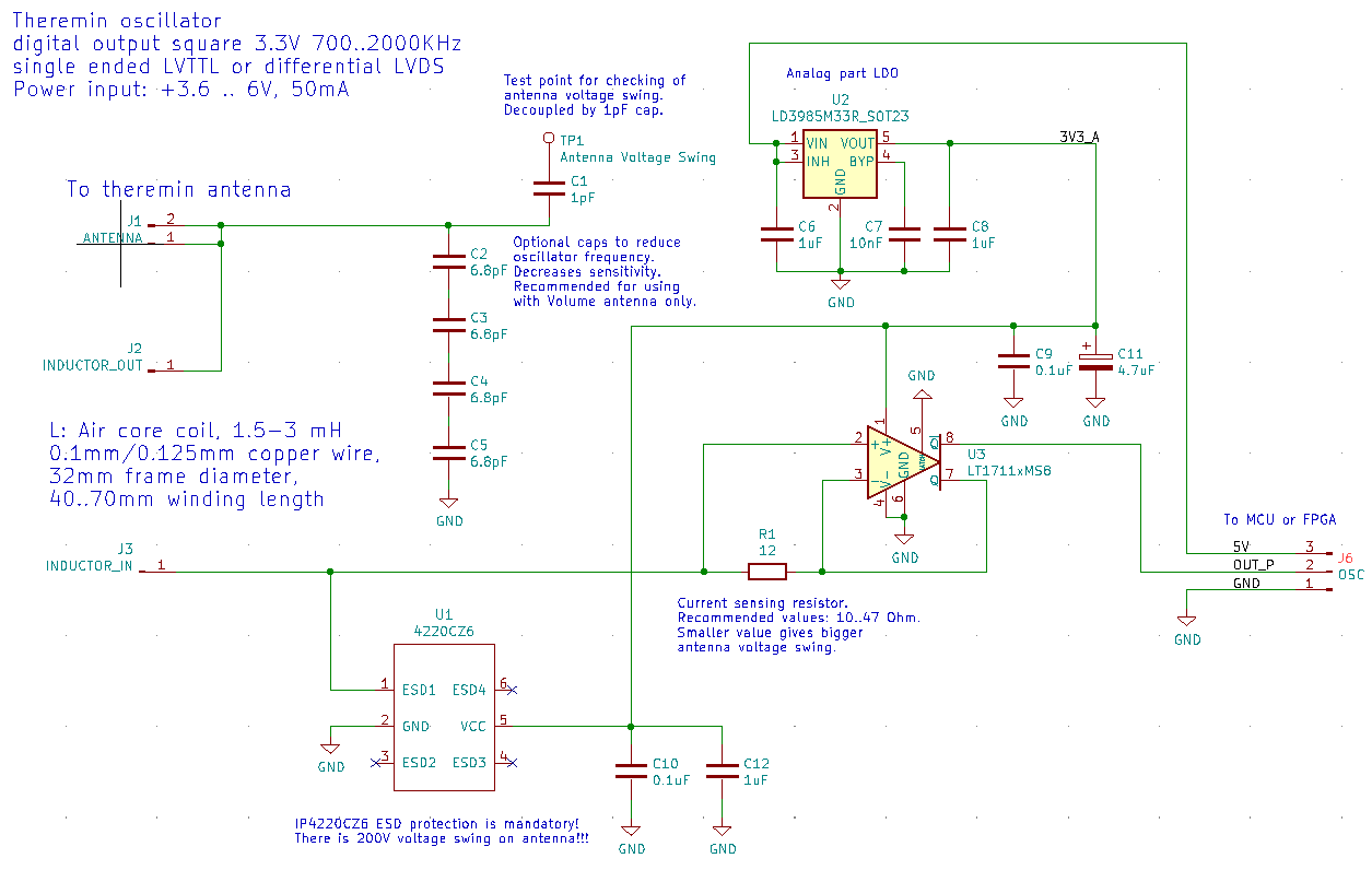
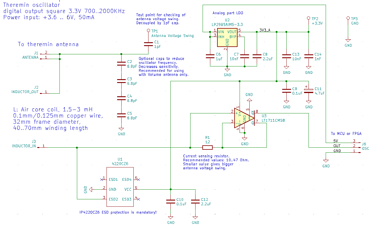
Finally found working comparator which can sense current of resistor on its own output.

All you need for oscillator are 2 components: LT1711 and resistor.
Of course, I forgot antenna and inductor.

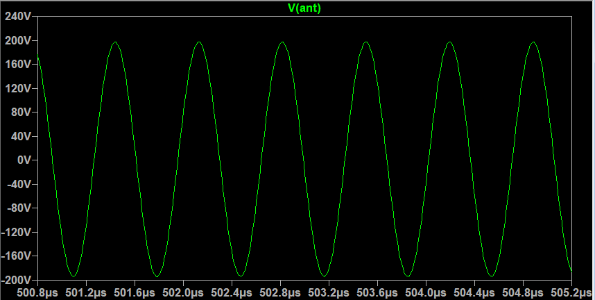
Simulation results in LTSpice: 1400Vpp antenna swing
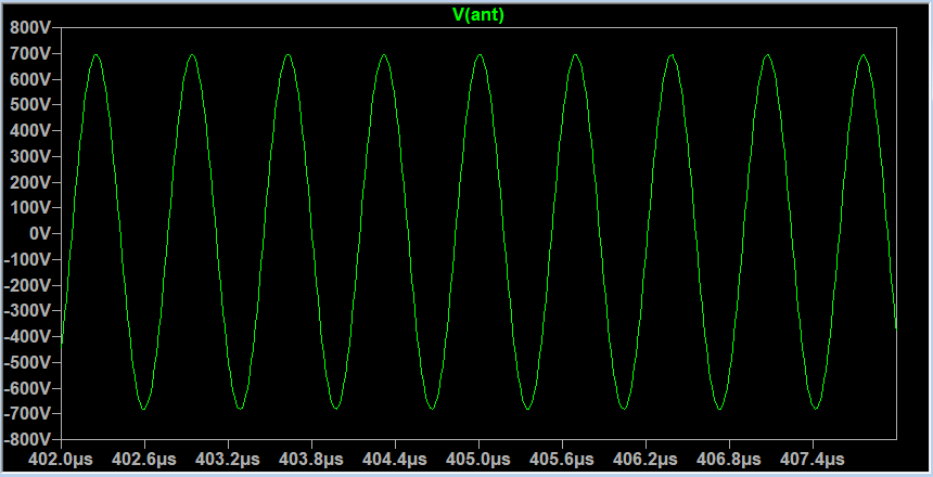

Sorry, it was with 12V power (max supported by LT1711)

Here is the same circuit powered from 3.3V: 400V antenna swing (with high R_serial inductor, can drop to 250Vpp)

LTSpice model:
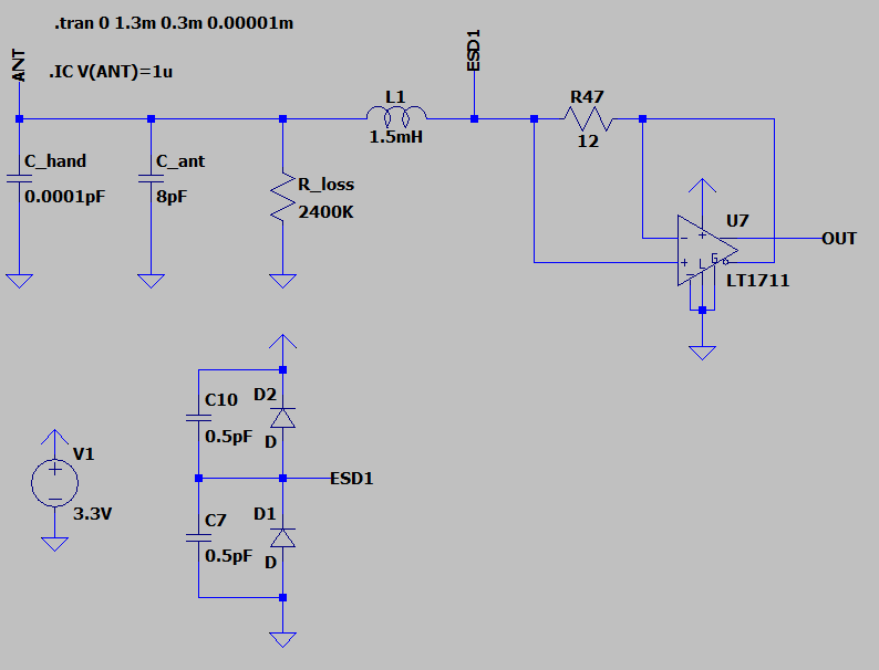

Download link of ltspice model file


Sensitivity (change of frequency for C_hand 0..1.5pF) is very high: (1452KHz-1332KHz)/1452KHz = 8.26%

Second (inverse) output can be used as square wave out.

Would be nice to check it on real hardware.

Posted: 10/22/2020 10:26:53 PM
dewster

From: Northern NJ, USA

Joined: 2/17/2012

"Would be nice to check it on real hardware."  - Buggins

I agree!  I would be very interested in stability, swing, and stalling.  It looks fantastic on paper!

IMO the best Theremin oscillators drive one end of the coil and have the antenna on the other end, and they really blast the coil with energy.  This one keeps the sensing low Z, though it does hurt the Q a bit.

Posted: 10/23/2020 12:43:06 AM
markallie

From: Madison, WI

Joined: 5/19/2016

Gentleman, (Dewster and Buggins) I am willing to layout and build PCB's with your design. The circuit seems simple enough. I would like to know what features you would like a PCB to have. What connectors or connection style would you like. Like for power, antenna etc. What possible possible variants would you be interested in. I can get 10 - 10cm by 10 cm PCBs for almost nothing In about a week. Let me know if you are interested. I can build them and send you some. Your sims seem to contain many parasitic impedances. Do you have a circuit that doesn't contain them or should I just not include what I think are parasitics?

Mark Allie

Posted: 10/23/2020 2:54:39 PM
dewster

From: Northern NJ, USA

Joined: 2/17/2012

"Gentleman, (Dewster and Buggins) I am willing to layout and build PCB's with your design. The circuit seems simple enough. I would like to know what features you would like a PCB to have. What connectors or connection style would you like. Like for power, antenna etc. What possible possible variants would you be interested in. I can get 10 - 10cm by 10 cm PCBs for almost nothing In about a week. Let me know if you are interested. I can build them and send you some."  - markallie

That's might neighborly of you Mark!  I wouldn't say no to a freebie!  Though the oscillator may or may not prove to be not stable enough for Theremin work.

I would make R47 through-hole to make it easier to experiment.  L1 will be entirely off the board, so one would just need a hole for the wire or post.  The ESD device Buggins uses is IP4220CZ6.  The LT1711 should be bypassed close to the power pins with 0.001uF and 0.1uF ceramic (you can read the datasheet for info).  A 3.3V LDO regulator would be nice, I use LP2950 with 4.7uF tantalum caps at the input and output pins to ground.

"Your sims seem to contain many parasitic impedances. Do you have a circuit that doesn't contain them or should I just not include what I think are parasitics?"

Everything except the LT1711, R47, and L1 are parasitic.  The ESD device simulation behavior is approximated via diodes and capacitors, so those are sort of parasitic too.

Posted: 10/23/2020 4:48:23 PM
markallie

From: Madison, WI

Joined: 5/19/2016

OK I'm working on it. Dewster do you want the 2N3904 version put on the board too. There is plenty of room and wouldn't get in the way of the LT1711 version. I can have an option to supply one or the other oscillator.

Would you like the output of either oscillator buffered in any way? Maybe a couple of transistors in a class AB configuration or an additional gate of some kind to isolate the critical outputs from possible damage.

Mark Allie

Posted: 10/23/2020 5:41:37 PM
dewster

From: Northern NJ, USA

Joined: 2/17/2012

"OK I'm working on it. Dewster do you want the 2N3904 version put on the board too. There is plenty of room and wouldn't get in the way of the LT1711 version. I can have an option to supply one or the other oscillator."  - markallie

I won't say no!  Knock yourself out!

"Would you like the output of either oscillator buffered in any way? Maybe a couple of transistors in a class AB configuration or an additional gate of some kind to isolate the critical outputs from possible damage."

I'm fine with not buffered, but Buggins may have some suggestions here.

Posted: 10/23/2020 6:11:14 PM
Buggins

From: Porto, Portugal

Joined: 3/16/2017

I've designed and routed PCB in KiCAD for LT1711 oscillator experiments.


It's a bit overcomplicated but allows to test a lot of options.
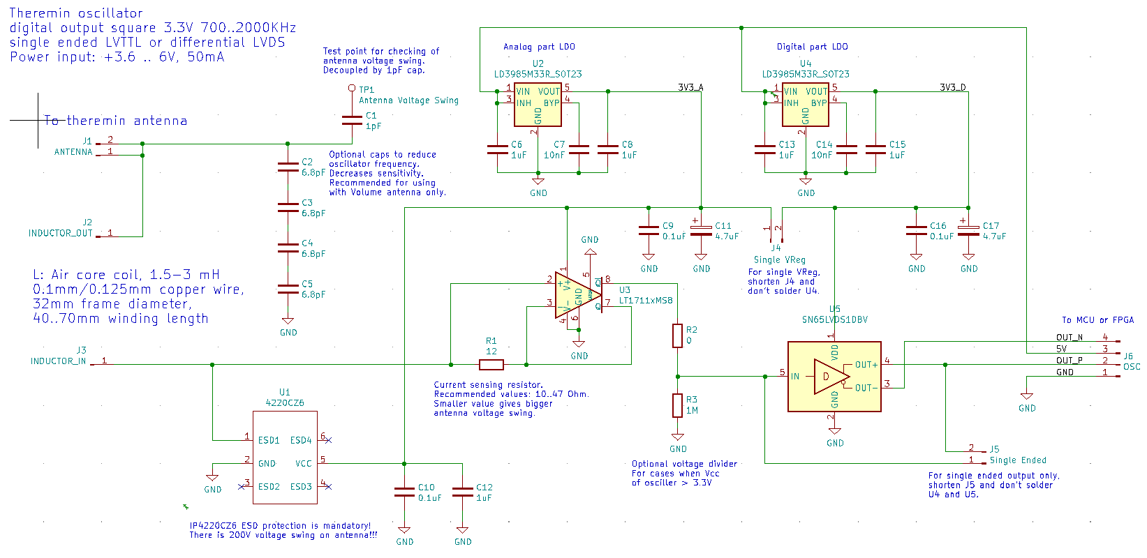
Optional LVDS output - don't solder and shorten J5 if not needed.
Optional higher Vcc for comparator (used only with LVDS output). When used - solder R2, R3 to divide voltage to 3.3V. If not used, R2 should be shortened.
Optional separate regulators - for oscillator and output. Mandatory when using higher voltage. Optional when oscillator is powered by 3.3V. Only one reg is needed for single ended output.
Some caps may be not soldered.
Optional capacitor chain from antenna to ground (e.g. to reduce frequency of volume antenna w/o big L).
Optional 1pF decoupling capacitor to measure antenna voltage swing.


PCB render top view:


PCB render bottom view:


Strange PCB layout - because it's intended to fit into 32mm plastic water pipe - frame of inductor. For out-of-tube usage, just solder vertical pin headers to use screw holes.


KiCAD project shared on github

Gerber files can be downloaded here

Simplified design - single ended output:


KiCAD project github link

Gerber files download link

Posted: 10/23/2020 9:30:21 PM
markallie

From: Madison, WI

Joined: 5/19/2016

Looks great Buggins. I'll stop my design. You might want to put R1 right on top of the input pins and put the bypass caps on the bottom of the board. That way you can use 1000pF, 0.1uF and a 4.7uF tant closely mounted to the power pins. I'm interested in the shield copper you are using around the input pins as well as the power ground copper. It's hard to see on the 3D image.

Mark Allie

Posted: 10/24/2020 5:20:30 AM
Buggins

From: Porto, Portugal

Joined: 3/16/2017


Looks great Buggins. I'll stop my design. You might want to put R1 right on top of the input pins and put the bypass caps on the bottom of the board. That way you can use 1000pF, 0.1uF and a 4.7uF tant closely mounted to the power pins. I'm interested in the shield copper you are using on around the input pins as well as the power ground copper. It's hard to see on the 3D image.

Mark Allie


Tank you for advices. I'm newbie in electronics, and will be glad to any help.

I've read datasheet and understood from PCB layout recommendations to route bypass caps in the same layer, w/o vias.
Maybe, I'm wrong.

Better view of copper layers:

There is no 1000pF cap.
There are only 4.7uF and 0.1uF bypass caps near comparator.
Other caps are far enough:  0.1uF and 1uF near ESD protection IC, and 1uF near voltage regulator.
Do you think it makes sense to add more caps with different C, like 1nF, 10nF?

I don't see where to put new caps on top side. In compact design below, they can be located on bottom layer, but not as near.


Trying more compact layout, with two bypass caps on bottom side.
Double vias of bigger size for both gnd and 3.3v from top layer comparator power pins to bottom layer bypass caps.
Added 1nF and 10nF optional bypass caps.
Traces for comparator are wider now.
Added 3.3V and GND test points.

Updated schematics:

Copper:

Renders:


Project and gerber files are overwritten under the same links:

KiCAD project on github

Gerber files download link

Posted: 10/24/2020 4:56:17 PM
markallie

From: Madison, WI

Joined: 5/19/2016

Buggins, This may be superfluous information but I will mention it anyway. You claimed to be a newbie but your layout looks better than what a newbie would produce. Good job.

The LT data sheet talks about using 1000pF (1nF), 0.1 uF and 4.7uF tant. Perhaps you already know this but in case you don't I want to say that 0.1uF is already getting high enough in capacitance that the self resonance frequency can be in the MHz and sometimes 10's of MHz. Self resonance is where the cap has an LC resonant peak and becomes inductive instead of capacitive. This doesn't allow for fast enough current injection into the comparator during high speed current needs like switching. This is where the 1nF comes in. The self resonant frequency is usually 1GHz or so. This gives the fast current the comparator needs to switch quickly. Unfortunately there isn't a lot of current (charge) available in a 1nF to maintain a sustained current draw. That's where the 0.1uF and 4.7uF tant come in.

I know it is a trade off between having the bypass caps on the top layer and the input lines short. With a comparator this fast I believe it is more valuable to have the R1 near the inputs and put the bypass caps on the bottom layer utilizing vias. The vias have a small amount of inductance which hurts high speed current pulses going from the cap to the chip. In my experience this trade off is usually the better one compared to putting R1 far away from the input pins. Far away is OK with good input shielding. I usually go for short input traces but you can do more shielding and make that work.

One thing that is important with a comparator this fast is shielding the inputs from the output. The fast "high" voltage output can affect the input signals. Usually there is a shield made up of GND and power. The recommendation is to use an isolated GND near the inputs that ties back to  the system ground at one point. This avoids high current flowing in the isolated GND shield. Usually the GND and power shields which ever you use are on both sides of the PCB. The GND pin (6) of the LT1711 has large current flowing in and out of it as it is related to the output. This pin should not be connected to the shield except through the single connection from the shield to the system ground.

Enough about comparators. This is not really about Theremins.

Mark Allie

You must be logged in to post a reply. Please log in or register for a new account.