Let's Design and Build a (mostly) Digital Theremin!

Posted: 7/18/2016 6:37:34 PM
dewster

From: Northern NJ, USA

Joined: 2/17/2012

Trying to read that patent but my eyes keep glazing over from all the gobbledygook.  It claims the MSb inverter is part of a high pass filter block, but that's incorrect.  The parallel data coming from a singly clocked LFSR is already ~differentiated if you consider it to be signed.  The inverter merely converts signed to unsigned.  IANAL, but I believe if you want signed and differentiated noise from an LFSR you can just use it directly (and sign extend it if necessary) and not infringe on the patent.  If you want unsigned you would need the inverter, but it's not clear to me as to how this would be infringement either, as inverting the MSb is a well known method of converting signed <=> unsigned.  Ugh, this shit just ties people's hands in nonsense.

One thing the patent mentions is the combination of uncorrelated noise samples leading to a triangular PDF (probability density function).  You get a rectangular PDF when you throw one die, because the probability for each value 1 thru 6 are the same.  You get a triangular PDF when you throw two dice, which is easily seen by listing all possible outcomes:

2 = 1+1
3 = 1+2; 2+1
4 = 1+3; 2+2; 3+1
5 = 1+4; 2+3; 3+2; 4+1
6 = 1+5; 2+4; 3+3; 4+2; 5+1
7 = 1+6; 2+5; 3+4; 4+3; 5+2; 6+1
8 = 2+6; 3+5; 4+4; 5+3; 6+2
9 = 3+6; 4+5; 5+4; 6+3
10= 4+6; 5+5; 6+4
11= 5+6; 6+5
12= 6+6

So you can see 7 is the most likely outcome, and 2 and 12 the least, with a linear slope to the probabilities on either side.  Triangular PDF works well for dithering audio, but applications like video and NCO / NCPD work best with a rectangular PDF.  Also, triangular dither requires an amplitude of 2 LSbs (post truncation), while rectangular dither only requires 1 LSb, so the injected noise with rectangular is lower.  Anyway, one can see how combining two independent noise sources might lead directly to triangular dither.

To get Gaussian PDF noise (not mentioned in the patent) you add together a bunch of (5 or more - more giving a better approximation) independent noise sources.  This gives a nice sinusoid, smoothing out the triangle above.  Gaussian noise is most similar to the noise generated by analog electronics.

The patent also uses the length of the LFSR to generate multiple samples at once, and to store previous values, which is neat but quite obvious - so what is really unique and patentable here?  To me it's exploitation of the otherwise problematic correlation of LFSR parallel samples separated by one clock.

Posted: 7/21/2016 7:48:16 PM
dewster

From: Northern NJ, USA

Joined: 2/17/2012

Investigating differentiated noise via spreadsheet, I was surprised to discover that straight 1st order differentiation of independent noise samples produces a triangular PDF.  I suppose I should have been prepared for this, as even though the use of each sample is spread over two successive time slots (first it is used as the main thing which gets the old thing subtracted from it, and then it is used as the old sample which gets subtracted from the new) the noise it gets combined with is itself independent, and independent combinations are like two dice, hence the triangular PDF.  Knowing this, it was not so surprising to find that higher order differentiation tends to Gaussian PDF. 

Things they don't teach you in school (and that don't instantly turn up in Google).  IIRC, my first encounter with the use of a multi-sample combination to produce Gaussian noise was in a physics lab in college - extremely basic and handy information that was nowhere to be found in any of my class texts.

Posted: 7/24/2016 8:49:10 PM
dewster

From: Northern NJ, USA

Joined: 2/17/2012

Rotary Encoders

(Mostly a rehash of this post.)

Busy bolting a bunch of System Verilog of stuff onto the processor. Got the NCPD, simple quadrature phase detector, and 4th order LPF tied together with a processor register interface.  Need to do the same with the SPDIF TX component and for some kind of serializer for the LED tuner.

I was planning on doing the rotary encoder debounce and decode in software, but now I'm wondering if throwing a tiny bit of hardware at it in order to conserve processor real time for bigger and better things might be a better approach.  I was thinking SW would be safest if glitching is a problem, as it could perhaps be dealt with more flexibly in SW, but as a first pass I'm going the HW route.  The pushbutton (when the encoder shaft is pressed) debounce is probably best being SW based, as it may need tuning.

The encoder hardware outputs form a 2 bit glitchy inverted Gray code, but only one input is supposed to glitch at a time.  Detent state is 11.  First thing is to synchronize the inputs with the system clock, and we do this with two shift registers, then we invert.  It's much simpler to feed the result to a state machine (SM) if we first convert the Gray code to binary, here the MSb is fed to the SM straight, while the XOR of the MSb and LSb form the LSb fed to the SM.  To see this:

CW rotation (inverted Gray): 11, 10, 00, 01, 11

Inversion (Gray): 00, 01, 11, 10, 00

Binary conversion: 00, 01, 10, 11, 00

A trick here is to use a 3 bit up/down binary counter as the state machine.  Detent position is 000, with CW rotation incrementing by 1 thus going positive, CCW decrementing by 1 thus going negative.  Machine transitions are limited to seeing an increment or decrement value at the input, and detent at the input always resets the state.  So if the machine has transitioned to +3 and detent is seen, we output a CW pulse.  And if the machine is at -3 with detent input, we output a CCW pulse:

CW state transitions: 000, 001, 010, 011, 000

CCW state transitions: 000, 111, 110, 101, 000

Even if doing this with SW we would need resynchronization, which takes at least 4 flops.  Doing it all in hardware (including resync) requires 12 LEs (logic elements), which is just a drop in the ocean even for the smallish FPGA we're targeting.  Each encoder needs a separate SM to track what's going on, and the processor register interface would likely be clear on read.

I suppose the moral here is to use the carry chain logic for state encode / decode if binary is (or can be made) a good fit to the state.

================

Also finalizing on system timing.  There's a 50MHz oscillator on the demo board.  Running this through one of the 2 configurable PLLs in the FPGA and multiplying/dividing by 29/236 gives 6.144067MHz.  For SPDIF we need 48kHz * 128 = 6.144MHz.  So the reference is 67Hz high, or +11pmm, which is within the 50MHz oscillator manufacturing tolerance limits. 

The SPDIF TX module has a 48kHz frame output which will be resynchronized and used as an interrupt for the one or more processor threads handling the capacitive DLLs, sound generation & filtering, as well as LED tuner output and rotary encoder sampling.

The second FPGA PLL will be used to drive the processor core at whatever maximum speed is fairly easily attainable (hopefully ~190MHz or so for 190 aggregate MIPS).

Posted: 7/28/2016 4:31:44 AM
dewster

From: Northern NJ, USA

Joined: 2/17/2012

Trying to figure out the TLC5916 via the datasheet (serializer and constant current driver for the LED tuner) and for the life of me it's all but impossible.  I've seen some lame datasheets in my time and this one is near the bottom in terms of describing what's really going on.  There's a rather odd way to place it in the mode where you can set the brightness and read diagnostic info, which they describe in various vague and vaguely different ways.  They show the latch as an independent clock in some of the diagrams, but then they give setup and hold to it from the serial clock?  The text states the output data is latched on the falling edge of the latch, but the edge to output spec is from the rising edge?  I'm going to have to breadboard it and send it some signals.  Independent clocks and asynchronous enables shouldn't have other modes where they behave as synchronous to some other clock.  Kind of surprisingly coming from TI.  </rant>

It's only slightly better than this joke data sheet.

[EDIT] Someone else crabbing about the TLC5916 datasheet, so it's probably not just me.  What's unsettling is the more time you spend poring over the datasheet the less sense it makes.  This IC should be one of the most straightforward things around but it's loaded with poorly documented cruft.  This seems to be a case of an analog team designing a fundamentally digital IC.  Analog is hard, but digital is deceptively harder than it seems to do right - simplicity, consistency, and adhering to rational interface norms are everything.

The TLC5916 is just a serial string of 8 flops - a simple shift register - driving a second layer of 8 flops in parallel, which drive the constant current outputs.  The serial clock shifts the serial data in and out.  Two other inputs control transfer from the serial flops to the parallel flops, and output enable.  The basic operation of these other two inputs is strange, and their overloaded functions are implemented in weirdly complex ways.  Even the current (brightness) setting is oddly implemented, with a discontinuity in the center and flipped endianness.

[EDIT2] Levenkay over at AVR freaks: "I finally took a look at the spec-sheet for that LED driver IC. Its interface is so totally botched that there must have been some enormous-volume customer who locked in on the unwieldy nightmare early for TI not to have corrected the design. Kind of like those oddball AVRs that have only twelve I/O pins, but are packaged in 294-pin hairbrushes, 'cause that's what General Motors ordered (I know, I exaggerate somewhat...). I would expect TI to offer a similar part, but with a sane interface that you could switch to; do they?"

I wish.  "Hairbrushes" <snerk>.

Posted: 7/29/2016 4:11:35 PM
dewster

From: Northern NJ, USA

Joined: 2/17/2012

TLC5916 - The Breadboarding

Yesterday I modified the Hive CLI (command line interface) to enable the interruption of individual threads.  Then I wrote a routine for thread 1 which takes four 32 bit values from memory and serially kicks them out over four FPGA pins.  This gives flexible and independent control over all the TLC5916 inputs: clock (rising edge), data, latch enable (active high), and output enable (active low), all conveniently triggered via interrupt.  Clock period is approx. 1.8us.

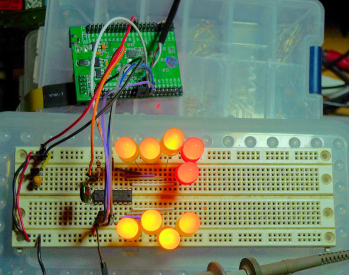
I stuck the TLC5916 on a breadboard with the FPGA demo board providing 5V and 3.3V via the USB serial cable.  Using the serial interface to Hive I can manipulate the CLI and therefore exercise the chip, and this can be automated via the TTL scripting language in the terminal program I'm using (Tera Term).  I've got 7 jumbo yellow LEDs connected to the chip, and two jumbo red LEDs in series hanging off the 5th output.  The LEDs are powered from the 5V supply, and the chip is powered off of 3.3V.  Here's a picture of my setup:

Test Results:

1. Two high brightness red LEDs in series can be powered off of the 5V LED supply.  This is good news because I was planning to do this on my Theremin tuner display board.  LEDs in series are more power efficient in this configuration.

2. LED[0] (hanging off of TLC5916 pin 5, nOUT0) lights when a single 1 is shifted in with a single clock, followed by the rise and fall of LE (latch enable).  This means the serial data in "normal mode" is MSb first.

3. The behavior of the latch enable is pretty odd.  Setting LE high and clocking in new data causes the continuous transfer of data from the serial flops to the parallel outputs, so it seems to be a transparent latch rather than a clocked flop.

4. Setting LE high and clocking a single high bit in and all the way through (nine clocks), I see all of the LEDs light very briefly and very faintly.  So control over LE (and/or OE) is essential for applications in which the LEDs need to be completely dark when off.

5. Since LE is a transparent latch, output data changes on the rising edge of LE.

6. The switch to special mode is accomplished by sampling OE (on the clock rise) high, low, high, with LE sampled high on the fourth clock rise.

7. Special mode data is sent LSb first!  The datasheet says OE must be high for special mode data shifting.

8. In special mode, with a 1k current set resistor, the maximum measured current is 19.54mA, the minimum is 1.634mA.  The datasheet says these should be 18.75mA and 1.575mA, so not too far off the mark.

9. The switch back to normal mode is accomplished by sampling OE (on the clock rise) high, low, high, with LE sampled low on the fourth clock rise.  The datasheet has a typo here.

10. Clock rise to data output on the serial data output pin 14 is around 18ns.  This could be problematic when cascading devices (data race, I've seen this before on real hardware).  They should have kicked the data out on the clock fall, though this could lower the top speed of the serial interface.  If you have extra controller pins you might consider feeding serial data to each device separately.

11. The LE high event which causes the switch to special mode doesn't actually latch data, and you can shift data in and out of the part during the switch to special mode - a latch at the end will latch the data into the brightness register.

12. Due to 11 above, you can shift brightness data in while doing the normal => special mode switch.  If you want to switch back to normal mode at the end the OE low for one clock can follow the LE event that latches the special data.  This requires 12 clocks.

Other:

In other fora, I've seen suggestions that OE be used for PWM brightness control.  That is possible, and PWM is more efficient than lowering drive current in an analog fashion, and PWM preserves color temperature.  But flashing a gob of LEDs on and off together will cause huge current spikes on the power supply lines.  For lower brightness it is probably best to do PWM on individual LEDs, that is turn only LED[0] on for a ms or so, then turn only LED[1] on or a ms or so, etc. which would keep the current load low and at roughly the same level over time.

It's interesting to see the difference between 20mA and 1.6mA drive.  Oh, you can definitely tell the drive is considerably lower, but it doesn't really seem 12 times lower (because of the non-linear response of the eye to light intensity).

Because LED forward voltage varies little with forward current, the IC should dissipate less when the drive current is lowered.  I didn't notice the IC getting hot or even warm during my testing.

I'm considering wiring all three TLC5916 devices in parallel, with separate LE drive for each.  This would provide an 8 bit interface to the processor.  Steering would be via two bits in the processor register.

Posted: 7/29/2016 6:23:56 PM
oldtemecula

From: 60 Miles North of San Diego, CA

Joined: 10/1/2014

Hey dew, nice to see some bread-boarding. Been installing my commercial breakout board for the first time this week because Valery S. is getting ahead of me in my own research. Him living in the town of Lev Sergeyevich Termen gives me inspiration. I need to get out of my Hive Seclusion and become more like a busy bee. laughing    Valery I will write when I get some results.

Christopher

Posted: 8/1/2016 8:05:52 PM
dewster

From: Northern NJ, USA

Joined: 2/17/2012

TLC5916 - SV Driver

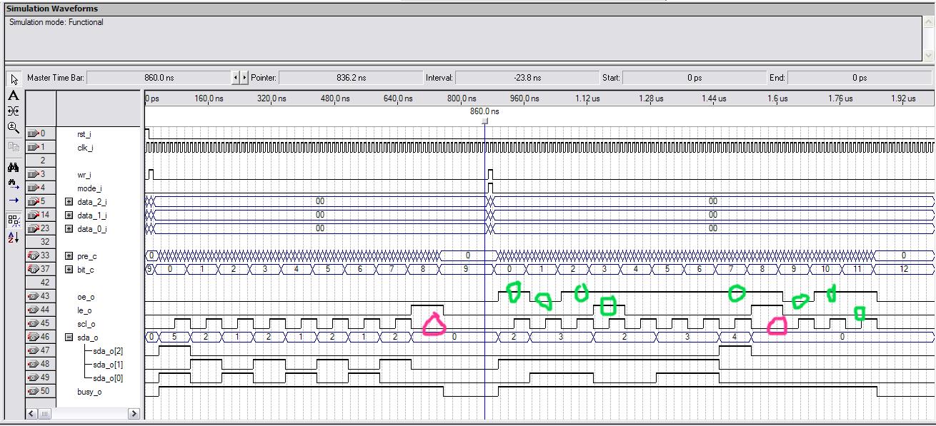
So how long can one badly designed chip take to examine and integrate into your setup?  The TLC5916 has taken me upwards of a week.  Because of the possible cascade data race, I decided to supply each of the three chips with data independently.  I also decided to parallel the rest of the control signals (clock, latch enable, output enable).  This allows a single state machine to feed all three chips at once, which shortens access cycle time, and allows the processor to write 24 bits of data at once and then go away until the next update is due (no bit camping / babysitting).  Finally, I decided to integrate mode switching into a separate cycle, where the mode is switched from normal to special, special data is transmitted, and then the mode is switched back to normal.  Special mode is specified by a register bit.  Here is a simulation of the System Verilog code:

The first transmission is in normal mode.  8 serial bits are sent LSb first with 8 serial clocks.  In the 9th clock position the clock is suppressed (red circle) and the latch enable is made high for that period, which latches the data into the LED select register.

The second transmission is in special mode.  Note the first group of green circles, where OE is sampled high / low / high and then LE is sampled high.  This puts the device in special mode during the transmission of data, and the LE is otherwise ignored here (latching is inhibited when LE is being sampled for mode switching).  Again at the 9th clock position the clock is suppressed (red circle) and the latch enable is made high for that period, which latches the data into the brightness register.  Previous to the latch the OE is sampled high, then after the latching event it is sampled low / high and then LE is sampled low, which returns the device to normal mode. 

Both of these cycles were confirmed to work via the breadboard & Hive & scripting exercise above, but I haven't integrated this HW driver into the Hive Theremin core yet.

I would prefer to have a more unified cycle, where the mode switching is always done at the start, but I didn't want to be flicking the OE unnecessarily when updating LED drive in normal cycles.  Normal cycles should overwhelming predominate, so it makes sense to cater to them.  The LED numbering is MSb first, but special data is sent LSb first, so I'll be numbering the LEDs opposite of that on the data sheet to make both accesses LSb first.

Even after ~20 years of designing FPGA hardware, I go round and round with implementation details re. these simple types of hardware drivers in SV.  This one started out two registers deep with a conventional state machine, but it was having trouble hitting 200MHz, so I made it three registers deep and employed the counter clock (prescaler) / bit counter as the state which worked out much cleaner and faster.

The TLC5916 seems to power up with the LEDs off, which is nice.  There is no direct control over OE via the processor register - the user can write all zero data in normal mode to turn them off.

Initially I didn't plan on doing this level of I/O hardware encode / decode for the Hive Theremin peripherals, but it makes sense as it should simplify the software and free up more real-time, and anyway there is hardware left over just sitting there.  These are actually the best kinds of co-processors because they're simple and relieve a lot of brain-dead SW activity.

Posted: 8/3/2016 4:02:36 PM
dewster

From: Northern NJ, USA

Joined: 2/17/2012

LCD Display

Even worse than the TLC5916 interface is the LCD display interface.  It seems to have originated with a really old CMOS process, so it runs really slow (really long setup, cycle, and hold times) - worse, you're talking to a super slow processor on the board that can only take data at a snail's pace.  There is a provision to run this parallel interface with 4 bits of data rather than 8, and it seems most people do this to limit interface pins.  The busy bit for the bus is unfortunately in a read register, so you can't just wire it to hardware, so it seems most people just wait for the longest time necessary for each instruction - which is hugely variable depending on the instruction!

Hardware power-on reset perhaps can't be trusted to put the display in a working state, and again there is no hardware wire for this, so there is a strange reset procedure which can be performed at the processor interface - during which time the busy bit is unreadable!  The reset procedure is strange in that you tell the processor that you want the 8 bit interface several times in a row (of course with different minimum times between each write) which is a pretty weird thing to be doing when you really want the 4 bit interface!  And the 4 bit accesses for this procedure are single nibbles rather than the paired nibbles of a byte, which makes it the odd man out and therefore one more thing that must be designed around.  (My conjecture is that the "set the interface to 4-bit mode" command is sticky and persists until another reset comes along, but the "set the interface to 8-bit mode" isn't.)

I really don't want to devote an entire processor thread to babysitting the LCD interface, so another custom SV hardware interface seems necessary here to compensate for yet another poorly designed peripheral.  I wonder how much engineering time is wasted worldwide on this kind of thing?

I've implemented a purely hardware interface to a two-line LCD display in the past in VHDL, but I've never experimented much with what's really going at the LCD interface beyond adhering to worst-case timing and such.  I don't believe there is an overall speed impact with running it in 4 bit mode, though there is perhaps the opportunity for nibbles to get jumbled.  Reset might be dealt with most simply by toggling power to the display, as I suspect that reset failures are mainly related to excessive power ramp times and glitching, and this might get one around the strange nibble writing reset procedure.  I'm thinking a 9-bit FIFO (command type bit + 8 bits of data) feeding a state machine which examines the commands coming out and adjusts cycle times accordingly (pretty much what I did before in VHDL, but simpler).

Beyond reading the SPLC780 datasheet, this is a really nice web site which discusses some of the tricky issues at this decidedly odd and sluggish interface: http://web.alfredstate.edu/weimandn/index.html.  I miss those old-school web pages where all you get is the facts.

Posted: 8/8/2016 5:07:26 PM
dewster

From: Northern NJ, USA

Joined: 2/17/2012

LCD Hardware

I'm probably overthinking this, but it's given me a reason to revisit some constructs and finally put them to bed.

Bus cycle timing in terms of setup & hold is likely somewhat dependent on the LCD controller logic supply voltage.  The wait after the cycle for the LCD processor to do it's thing may also be supply voltage dependent, but more indirectly because it is based on the on-board RC oscillator.  So I decided to decouple the cycle and wait timing.  If you do some math on the datasheet timing values, it seems the wait time for a normal instruction is 10 clocks, and the wait for a long instruction (screen clear, cursor home) is 40 times this.  RC minimum frequency is 190kHz, so normal cycle max wait is 10/190kHz = 53us, and long cycle is 40*53us =  2.12ms. (!)

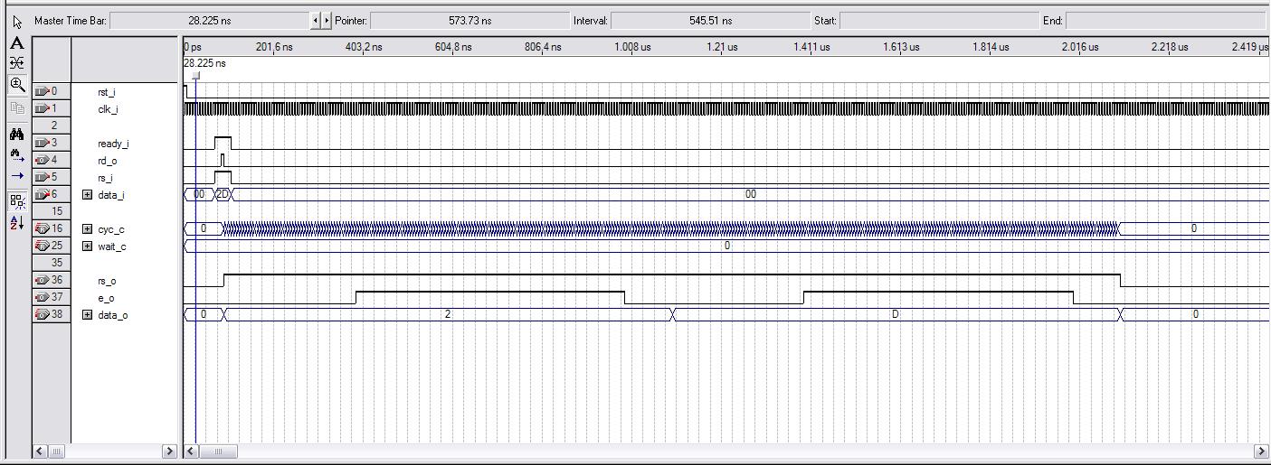
The bus sub cycle is defined by setup time, enable time, and hold time.  The total of these set the per nibble time, so two sub cycles are needed to transfer a byte.  Bus cycle times are ~1us per nibble, which is a drop in the bucket compared to wait times.  So it doesn't make a lot of sense to aim for minimum bus cycle timing as it doesn't net you much.  And with 1us inter-nibble timing we can give the setup and enable times lots of extra margin without impacting the overall access time by much at all.

The bus cycle setup, active, and hold times are given in the code as separate parameters in ns.  After the nibbles are transferred the wait timer starts, and this is based on a direct digital frequency synthesis (DDFS) component which gives a rough approximation of the 190kHz as the time base.  10 edges for a normal cycle, and 400 edges for a long cycle.  So all of the cycle times are based on the FPGA system clock, some hard timing numbers, and a derived clock, all of which can be independently set but that track together via the parameter math.

The above shows the bus cycle portion of an LCD access.  Ready will come from the not-empty output of a FIFO, read will do a FIFO pop.  RS is an extra data bit from the FIFO, giving 9 bits total.  Setup time for RS & data are the same here 300ns, enable time is 600ns, and hold is 100ns to make the full 1us nibble cycle.  The most significant nibble is presented first, the least significant second.  After this the wait timer starts and continues for a long time off to the right (not shown).

I worked on my FIFO construct, I had to make pointer protections optional and then disable them in order to get the speed up.  The external logic will safely access the FIFO, so pointer protections aren't necessary.  The other construct I worked on was the DDFS component.  The parameters now take input and output frequencies as reals (floating point values) and use the given phase increment width to ensure a worst-case level of precision.  DDFS is also used for the UART baud clock.

So I need to connect a FIFO and Hive register to this, stick it in the core, and see what it does on the breadboard.  Not sure if the 4 line x 20 char LCD I bought will work (had to solder a voltage shifter onto it as they sent me the 5V version).  LCD modules don't do anything when you power them up, which seems kinda dumb to me.  A self-test pin or something would be a very welcome addition.

Internally the design uses a direct form 5 state machine, two counters, and the DDFS component.  LCD interface timing is so long and sloppy compared to the system clock that internal delays and such are moot, which really simplifies things.

Posted: 8/10/2016 9:19:28 PM
dewster

From: Northern NJ, USA

Joined: 2/17/2012

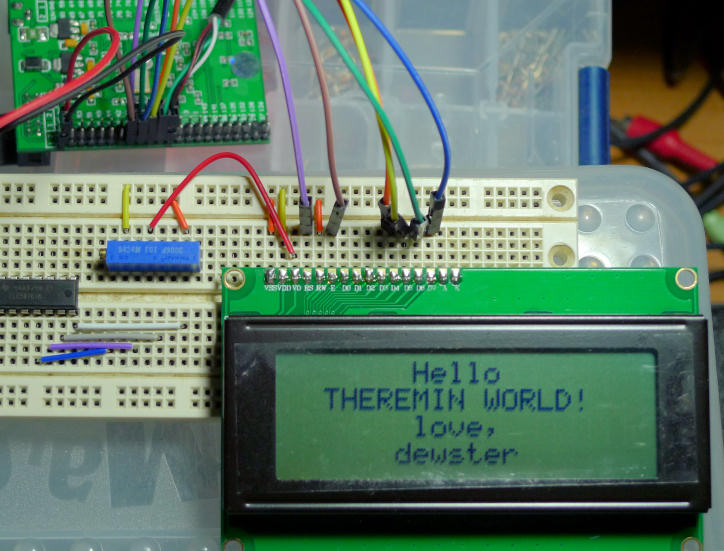
Got the LCD interface running a little bit ago, added Hive command line access to the LCD register:

Display looks a little skanky because I haven't removed the scuffed up protective plastic adhesive thingy.  No backlight is on here either.  Initialization and text provided via a TeraTerm script.  Ran first time right off the bat!

You must be logged in to post a reply. Please log in or register for a new account.