FPGA programming progress update.
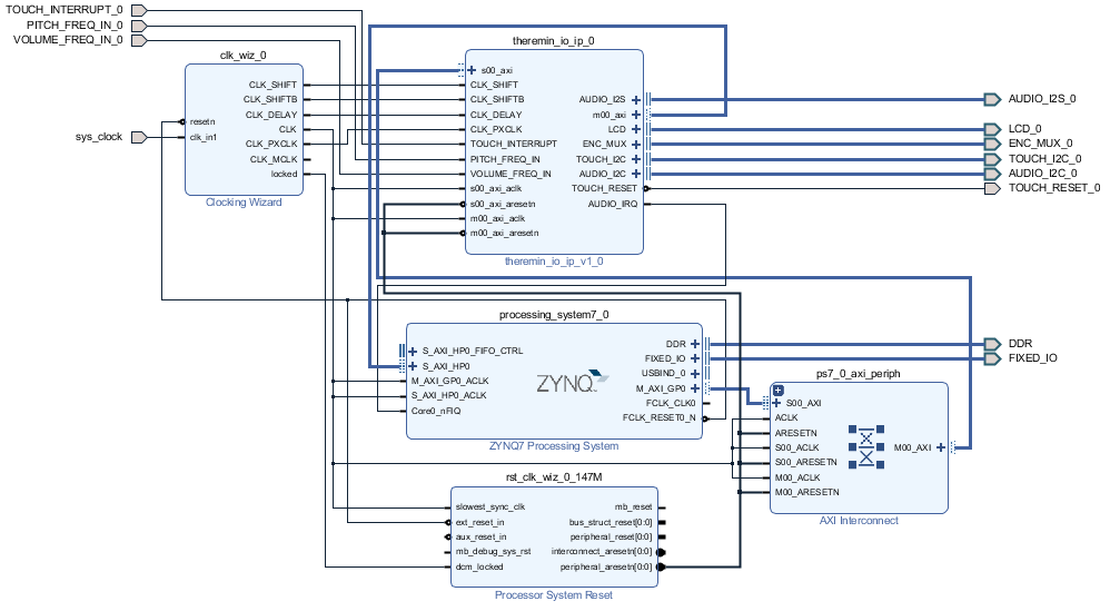
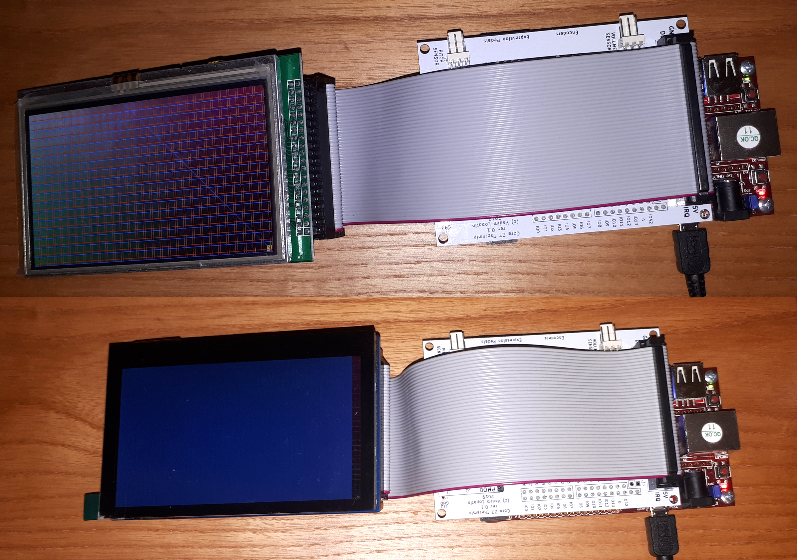
Created IP which combines theremin sensor, LCD controller, encoders controller, audio controller, two i2c interfaces.
(Missing components: sd_card, ADC for pedals board)
Created block design:

Utilization:
Code:
+----------------------------+------+-------+-----------+-------+
|          Site Type         | Used | Fixed | Available | Util% |
+----------------------------+------+-------+-----------+-------+
| Slice LUTs                 | 1317 |     0 |     17600 |  7.48 |
|   LUT as Logic             | 1217 |     0 |     17600 |  6.91 |
|   LUT as Memory            |  100 |     0 |      6000 |  1.67 |
|     LUT as Distributed RAM |   40 |     0 |           |       |
|     LUT as Shift Register  |   60 |     0 |           |       |
| Slice Registers            | 1638 |     0 |     35200 |  4.65 |
|   Register as Flip Flop    | 1638 |     0 |     35200 |  4.65 |
|   Register as Latch        |    0 |     0 |     35200 |  0.00 |
| F7 Muxes                   |   13 |     0 |      8800 |  0.15 |
| F8 Muxes                   |    0 |     0 |      4400 |  0.00 |
+----------------------------+------+-------+-----------+-------+
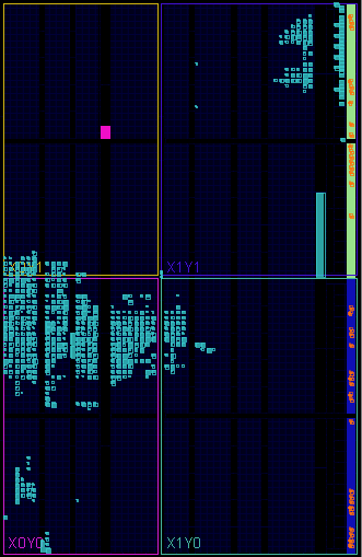
Placement on device (used cells are cyan):

Part of resources is occupies by AXI bus support blocks (interconnect, clock gen, etc).
Theremin IO IP itself takes 925 LUTs and 1177 registers.
I hope up to 90% of FPGA resources may be used for future advanced synthesizer implementation.
