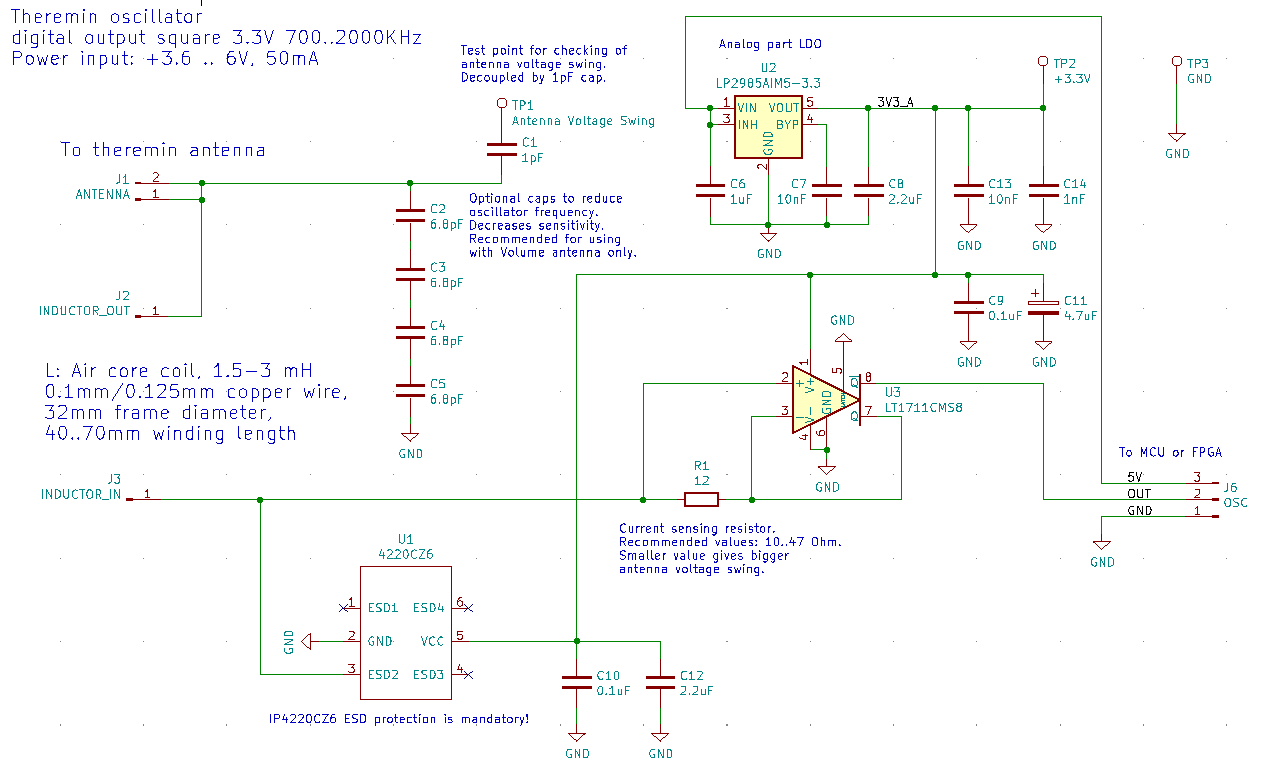
Awesome idea with resistor current sensing!
How fast you checked it on a breadboard.
Tried to find some comparator which could replace your BJT differential amplifier.
Most of components from LTSpice library do not work or have strange behavior.
Finally found working comparator which can sense current of resistor on its own output.
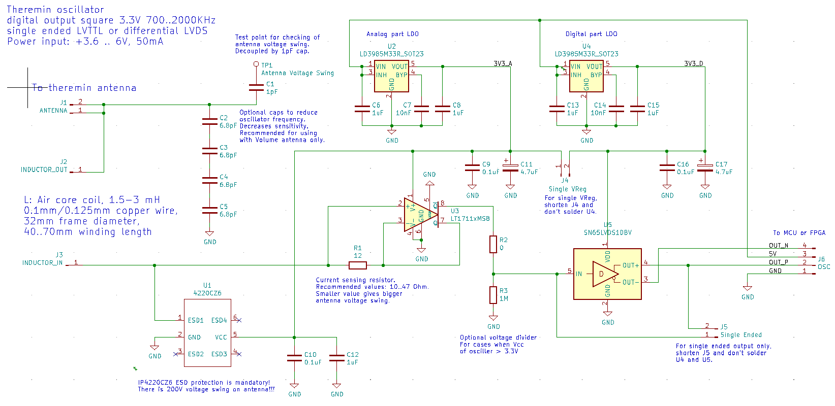
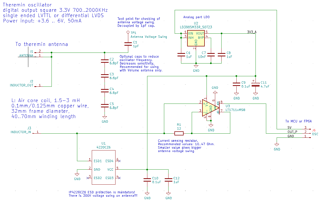
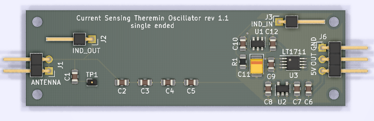
All you need for oscillator are 2 components: LT1711 and resistor.
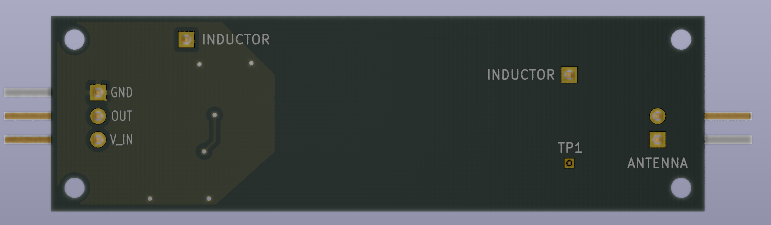
Of course, I forgot antenna and inductor.
Simulation results in LTSpice: 1400Vpp antenna swing
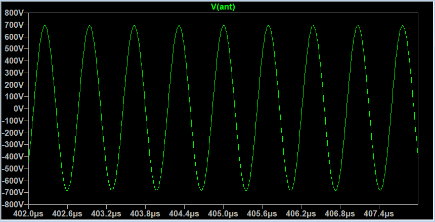
Sorry, it was with 12V power (max supported by LT1711)
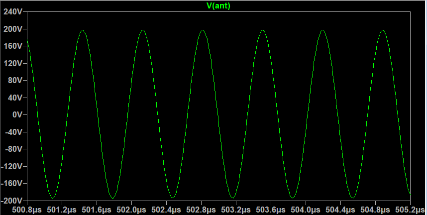
Here is the same circuit powered from 3.3V: 400V antenna swing (with high R_serial inductor, can drop to 250Vpp)
LTSpice model:
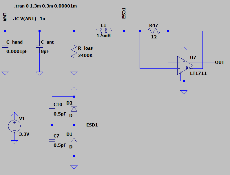
Download link of ltspice model file
Sensitivity (change of frequency for C_hand 0..1.5pF) is very high: (1452KHz-1332KHz)/1452KHz = 8.26%
Second (inverse) output can be used as square wave out.
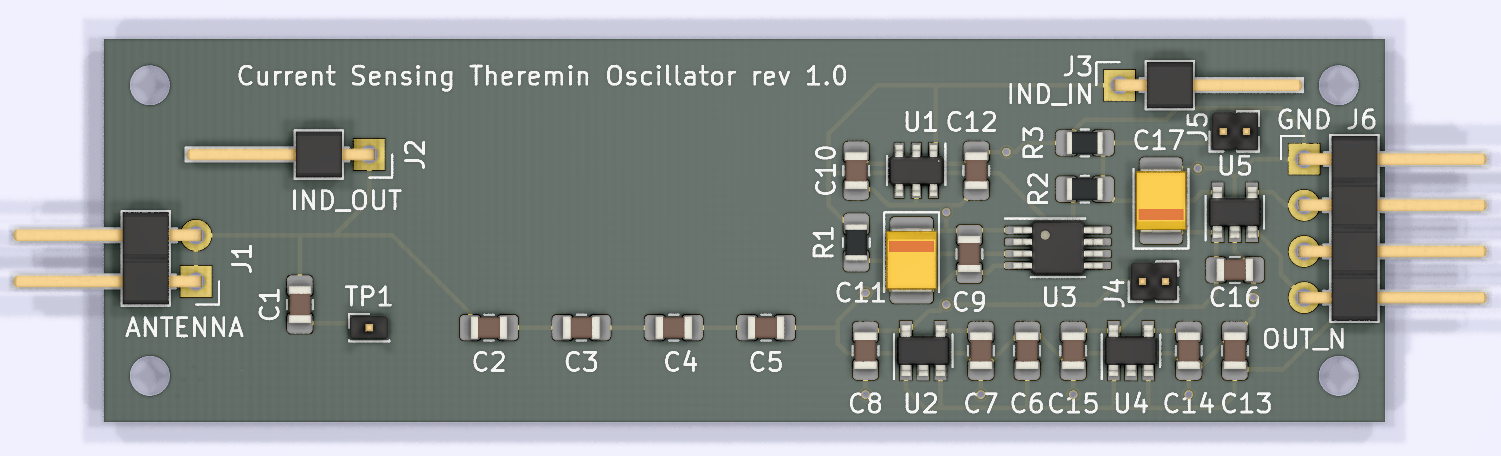
Would be nice to check it on real hardware.