Thank you, Mark!
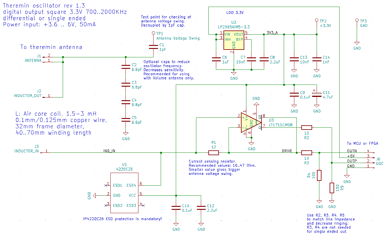
So, putting all bypass caps on bottom side seems ok.
I wanted to ask if order of caps in chain does matter, but it looks like you already answered. Lower value capacitors should be connected with shorter path to IC pins, while larger can be located at bigger distance.
Better design would have isolated island surrounding comparator and its bypass caps with two entry points.
Filling top area with Vcc instead of GND may form small but fast bypass cap on power line.
Next time I will try to take it into account. I will correct it in next revision of this PCB.
Meanwhile, I've already ordered manufacturing of PCBs using recent layout I've published.


