


Wow. That looks really impressive!
Let's design and build cool (but expensive) FPGA based theremin
Posted: 6/11/2021 7:11:53 PM

Gorgeous! Vadim, whatever they're paying you, you deserve a raise! :-)
[EDIT] "Going to search for 3D models and order 3D printing of knobs." - Buggins
It's one more thing to learn, but maybe get an Ender 3 or clone and play with OpenSCAD or similar. I've got a nice (IMO) parameterized knob pattern I can give you. You can't 3D print everything, but sometimes it's fairly amazing what you can print. Roger sent me a pitch arm that you'd swear was commercially made, dude's totally mastered the medium.
Posted: 10/14/2022 5:41:18 AM

Found interesting new FPGA board from Sipeed - Tang Primer 20K.
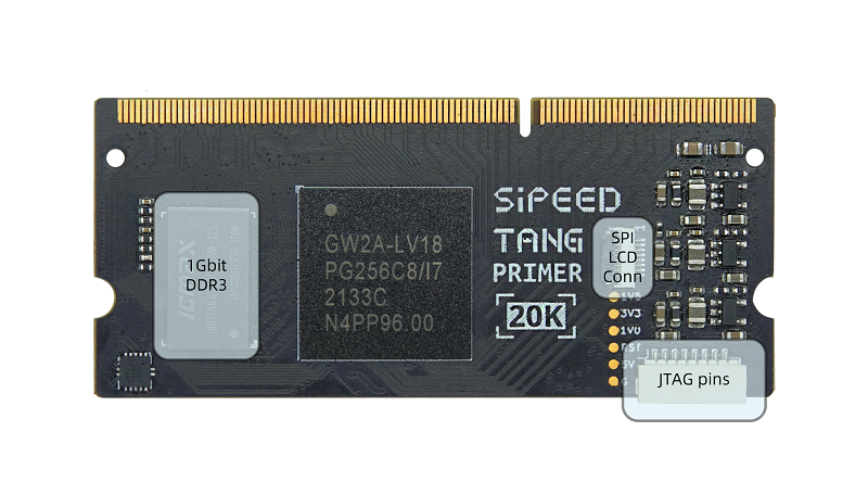
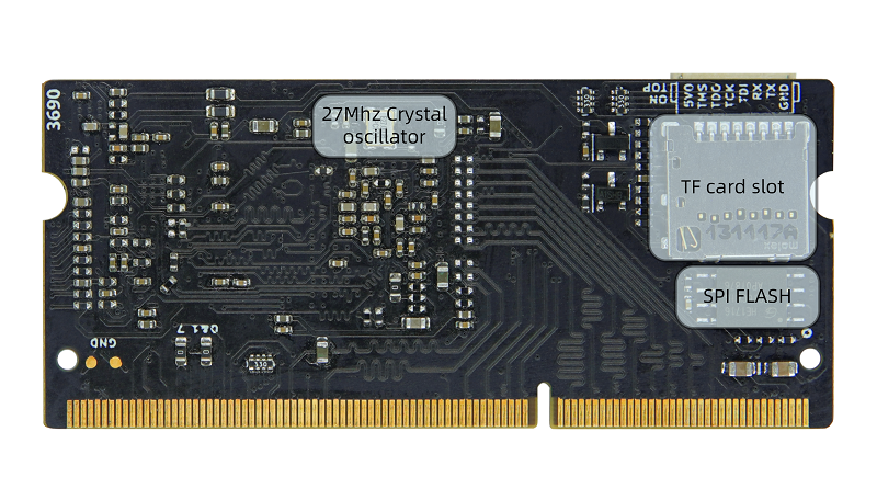
It's Gowin GW2A-LV18PG256C8/I7 FPGA based small core board in DDR3 SODIMM (204P) form factor and it's minimalistic - just FPGA chip, 128MB DDR3 with 16-bit interface, SPI flash, JTAG connector, SDCARD slot, FPC SPI connector (mainly for connecting SPI display).
It looks like it's new board, and became available only in September.
Additonal boards:
RV debugger (USB to JTAG board) - to program using on-board jtag connector.
Extension Board Lite - mainly SODIMM to 100-mil pins (2x 40x2 + 4x 6x2 PMOD) breakout, may come with or w/o pin headers soldered.
Big extension board - with a lot of interfaces like USB, HDMI, LCD display, camera, ethernet, etc. Not sure if it's already available to order.
Available in Sipeed store on Aliexpress
EUR41.36 - with lite core board w/o pins soldered
EUR42.7 - same with 40x2 pins and 4 PMOD connectors soldered
EUR28.69 - core board with jtag connector cable
EUR32.7 - core board with RV debugger, jtag cable and USB cable
Lite extension board w/o pins looks great for DIY projects - you can solder pins pointing down.
As well you can just solder SO-DIMM connector on your PCB and use core board directly - but it's harder to solder.
Available resources should be enough for digital theremin.
20K LUT4, 15K FFs (on gowin platform, only 3 of 4 LUTs have FFs)
46 BRAMs (1k x 18bit / 512 x 36bit) - about 100KB in total.
4 PLLs
117 I/O pins available, most of them support true LVDS with support of internal terminating R100 resistors (i'm keeping in mind idea to connect sensor front ends using differential LVDS lines to minimize noise).
48 18x18 multipliers
Using of 128MB DDR3 chip at 800MHz may eat up to 2K LUTs for memory controller IP, but there is open source alternative - small but slow.
IDE is a bit strange, similar to one from Lattice.
IDE version I've downloaded doesn't have simulator. It looks like usually Synopsys simulation tools are being used with gowin.
With LVDS capable FPGA, it's possible to use low noise interface to theremin sensor analog front end.
I hope it would decrease noise introduced by both transmission lines and power supply.
Let's use current sensing approach proposed by Dewster, with digital PLL part inside FPGA.
AFE will have one LVDS diff pair input (drive), and two LVDS diff pairs for output - reference and sensing.
Differential LVDS drive signal from FPGA to AFE - received by LVDS receiver.
Receiver output is used directly to drive LC tank via current sensing resistor R_sense.
Reference signal - drive signal (before current sensing resistor R_sense) is sent back to FPGA using LVDS transmitter.
Sensing comparator - measures sign of current through R_sense by comparing voltage on R_sense, and sends result of comparision to FPGA via LVDS differential pair.
FPGA based PLL should measure phase shift between reference (delayed copy of drive signal) and sensing signals, and adjust drive signal frequency to keep phase shift near 0.
Estimating analog front end cost (LVDS I/O, current sensing)
LVDS transmitter: ADN4661 EUR 2.87 on mouser EUR 3 digikey.pt
LVDS receivers: ADN4662 EUR 2.87 on mouser EUR 3 digikey.pt
Comparators with LVDS output: ADCMP604 EUR 6.84 on mouser EUR 9.07 digikey.pt
Total cost for 3 ICs: ~EUR 15.
A few additional cheaper components will be needed - power supply regulators, decoupling caps, sensing resistor.
Posted: 10/15/2022 2:29:44 PM
Vadim, thanks for the interesting pointers!
I'm at something of a crossroads with the D-Lev. I can maybe get more of the FPGA boards for $90 each, or a board that is similar (but different pinout) for $40 each. The original just seems way overpriced, though it would be a no-brainer. The similar board would require a re-spin of the main PCB, which is more work and risk for no real improvement. I guess I'm a bit weary from the sketchy availability and sky high prices, and the lack of control over the beating heart and peripherals. And I'd like to keep improving things, adding reverb and better support for physical synthesis, but the FPGA real-time and BRAM resources are largely consumed.
I'm quite wary of low quality tooling and simulation, and so am not at all anxious to move to another FPGA. A blend of processor and FPGA would be the most ideal I think. I've encountered a small batch of AFE hex inverters that won't oscillate unless the antenna is touched, which is disturbing. The encoder wiring is quite laborious, and the conditioning should be in SW rather than FPGA HW.
The ideal solution would be to get someone like JLCPCB to do the PWBs and populate all the components, but they only have one EP4CE10F17C8N in stock, and they want $143 for it!
Posted: 10/16/2022 6:19:13 PM
Eric,
Rerouting of main board, keeping support for different board revisions, etc. is a hard and error prone.
Of course, keeping the same architecture, and even FPGA chip, makes it safer.
I've tried to check what cheap boards are available.
Many of boards I seen year or two ago out of stock in online stores, or just disappeared from aliexpress search output.
I was planning to use some cheap enough Zynq board (a lot of FPGA resources, CPU, SDRAM controller is in CPU and you can just access it using DMA bus instead of spending a lot of resources for SDRAM controller... But the only cheap board with good pinout left is one from qmtech, which is reported on forums as having bad decoupling, badly traced, SDRAM is working only at half of expected speed...
Since new Sipeed Tang board just appeared, I hope it would be available at least for several years.
FPGA chips on mouser/digikey, are often out of stock or very expensive. Last time I checked there were no Lattice FPGAs in stock at all. But gowin chips were available, with reasonable price.
Surprisingly, boards from sipeed are cheaper, than FPGA IC price for one piece.
One more pro for trying new exotic arch is that it supports LVDS on 3.3V banks.
Xilinx starting with Series7 doesn't support LVDS anymore with 3.3V banks (Spartan 6 supported it).
Your EP4CE10 seems to have only ~10K LEs... Are there hand-solderable Cyclones with bigger resources?
It looks like 20K chip in new tang board has x2 times more LEs, DSPs, BRAM.
I've tried to play with gowin architecture. It looks similar to lattice (some are pin-to-pin compatible).
Found some useful information about simulations support in Gowin IDE. After synthesis and place and route, it generates netlist files for behavioral and timing simulation, which could be used by external tools to run simulation. Primitives library for both timed and behavioral simulation is available as well.
I'll try to find out how to use it.
Another possible way to simulate parts of project - write it in platform independent style, and then simulate on Vivado I'm familiar with.
As a test, I wrote ALU + 32x32 multiplier (with signed/unsigned mode for each operand, 4 shift modes for result for low 32 bit, hihg 32 bit, 16 and 24 bit right shift with overflow/underflow detection for FP16.16 and FP8.24 multiplication) in cross platform way (w/o using of platform primitives).
Multiplier has been inferred correctly from my code.
4-stage pipeline for multiplier and for ALU is running on 230MHz according to static timing analysis, which is not as bad as I expected.
But on Xilinx platform, similar ALU was able to run at 330MHz and consumes x3 times less resources (actually, single DSP module on xilinx can do most of work).
LUT4 arch comparing to LUT6 one consumes much more resources.
E.g. 4:1 MUX eats two LUTs per bit.
Another finding: SystemVerilog is not supported on gowin platforms. Only verilog and vhdl are supported.
P.S: did you ever try to order PCB assembly on JLCPCB? Is it expensive if only 5-10 boards are ordered? What is cost of soldering?
Posted: 10/18/2022 10:35:08 AM
"Many of boards I seen year or two ago out of stock in online stores, or just disappeared from aliexpress search output." - Buggins
Yes, it's fairly discouraging.
"I was planning to use some cheap enough Zynq board (a lot of FPGA resources, CPU, SDRAM controller is in CPU and you can just access it using DMA bus instead of spending a lot of resources for SDRAM controller... But the only cheap board with good pinout left is one from qmtech, which is reported on forums as having bad decoupling, badly traced, SDRAM is working only at half of expected speed..."
And it's a kind of Murphy's Law, anything you can't control in a project will go wrong.
"Since new Sipeed Tang board just appeared, I hope it would be available at least for several years."
Most of the newer boards seem geared to those wanting to experiment with the RiscV soft processor, and cameras, and LCDs. Making any of the I/O banks lower voltage kinda takes them out of the running for other hobby use too.
"FPGA chips on mouser/digikey, are often out of stock or very expensive. Last time I checked there were no Lattice FPGAs in stock at all. But gowin chips were available, with reasonable price."
One-off FPGA prices are insane, you can buy them on a board from China, postage and all for way less (if you can find them).
"Surprisingly, boards from sipeed are cheaper, than FPGA IC price for one piece."
This is the way it's always been, bulk purchasing drives the price way down, I saw it where I worked too, giant FPGAs for like $25, and this was 15 years ago. It's annoying, and one more way the little guys get locked out.
"One more pro for trying new exotic arch is that it supports LVDS on 3.3V banks."
Maybe forget LVDS? Just capacitively couple to one of the FPGA pins, use inverted feedback from another pin with a resistor to keep it centered?
"Your EP4CE10 seems to have only ~10K LEs... Are there hand-solderable Cyclones with bigger resources?"
Even if there were, I couldn't possibly buy them for a reasonable price.
"It looks like 20K chip in new tang board has x2 times more LEs, DSPs, BRAM."
That's encouraging! I wonder how much power it would draw with two Hive processors running in there? Mine is pulling ~0.5A and I wouldn't want to go much higher than that due to heat and USB limitations.
"I've tried to play with gowin architecture. It looks similar to lattice (some are pin-to-pin compatible).
Found some useful information about simulations support in Gowin IDE. After synthesis and place and route, it generates netlist files for behavioral and timing simulation, which could be used by external tools to run simulation. Primitives library for both timed and behavioral simulation is available as well.
I'll try to find out how to use it."
IMO if the FPGA toolchain fights you at all it isn't worth it the fight, but you seem to have more energy than I do for this stuff.
"Another possible way to simulate parts of project - write it in platform independent style, and then simulate on Vivado I'm familiar with.
As a test, I wrote ALU + 32x32 multiplier (with signed/unsigned mode for each operand, 4 shift modes for result for low 32 bit, hihg 32 bit, 16 and 24 bit right shift with overflow/underflow detection for FP16.16 and FP8.24 multiplication) in cross platform way (w/o using of platform primitives).
Multiplier has been inferred correctly from my code."
The Hive 33 x 33 = 65 multiplier is hand-written too, and can only do ~200MHz on a good day. I worked on it quite a bit to get it there. When it's in a sea of other logic it has a hard time hitting 180MHz.
I'm curious why you might want to use reduced resolution FP ops? Fixed point (where the result is the upper 32 bits) multiply works really well for filters, oscillators, etc.
"4-stage pipeline for multiplier and for ALU is running on 230MHz according to static timing analysis, which is not as bad as I expected.
But on Xilinx platform, similar ALU was able to run at 330MHz and consumes x3 times less resources (actually, single DSP module on xilinx can do most of work)."
Yes, hardware connected hardware will always win by a wide margin.
"LUT4 arch comparing to LUT6 one consumes much more resources. E.g. 4:1 MUX eats two LUTs per bit."
It took a while for Altera and Xilinx to come up with LUT6, I guess because 6 isn't a power of 2 and it tends to strand logic, but it makes sense.
"Another finding: SystemVerilog is not supported on gowin platforms. Only verilog and vhdl are supported."
That's kinda a deal killer for me. So many features in SV are sweet, like the packaging system. Though often when they say they don't support SV, they're saying they don't fully support it for synthesis, which no one really does anyway, as some language constructs don't apply.
"P.S: did you ever try to order PCB assembly on JLCPCB? Is it expensive if only 5-10 boards are ordered? What is cost of soldering?"
No, never done it, though I should give it a go if the D-Lev project ramps up anytime soon. I don't mind soldering a bit, but hunched over a hot iron for days on end isn't super pleasant.
Ah, I'm Mr. negative vibe merchant lately, please ignore me!
Posted: 10/18/2022 7:52:16 PM
Maybe forget LVDS? Just capacitively couple to one of the FPGA pins, use inverted feedback from another pin with a resistor to keep it centered?
Just trying to keep possibility to experiment with more noise immune AFE.
The Hive 33 x 33 = 65 multiplier is hand-written too, and can only do ~200MHz on a good day. I worked on it quite a bit to get it there. When it's in a sea of other logic it has a hard time hitting 180MHz.
More interesting thing here is that hardware multiplier itself is reported by static timing analyzer as supporting max 350MHz.
230 MHz limit comes from other logic.
I'm curious why you might want to use reduced resolution FP ops? Fixed point (where the result is the upper 32 bits) multiply works really well for filters, oscillators, etc.
It's to support fixed point values > 1.0 Doesn't it make sense? How do you deal with overflows?
Actually, additional 2 shift modes consume big enough resources (64 LUTs). As well, overflow detection has its price. If you are suggesting that it's useless, I will drop it.
That's kinda a deal killer for me. So many features in SV are sweet, like the packaging system. Though often when they say they don't support SV, they're saying they don't fully support it for synthesis, which no one really does anyway, as some language constructs don't apply.
They support .sv extension. But I've tried keywords like logic, always_ff, etc. -- SV really does not work with gowin synth.
Posted: 10/18/2022 8:44:21 PM
"Just trying to keep possibility to experiment with more noise immune AFE." - Buggins
An excellent and worthy goal! Though the RC time constant of C coupling with negative feedback R could be kept small, like 10 cycles or so. It's a weird scenario because the signals aren't traveling all that far, but the distance isn't negligible either. Probably the most interference comes from the I/O bank bouncing around, and thus the threshold voltage doing the same, which differential I/O should mostly fix. I really mainly only see this type of interference though when the bank VCC droops below the voltage regulation point (due to flaky USB extension / dongle connection).
"More interesting thing here is that hardware multiplier itself is reported by static timing analyzer as supporting max 350MHz. 230 MHz limit comes from other logic."
That's really fast! IIRC the Altera BRAMs have a fairly low upper limit like that, even if registered.
"It's to support fixed point values > 1.0 Doesn't it make sense? How do you deal with overflows? Actually, additional 2 shift modes consume big enough resources (64 LUTs). As well, overflow detection has its price. If you are suggesting that it's useless, I will drop it."
There are a couple of cases in the D-Lev SW where a mult > 1.0 happens, the knee strength is one of them. If you can take a bit of a resolution hit then you can just shift and clamp after the multiplication. Otherwise the integer and decimal can be dealt with and added together, and then clamped. Filters, oscillators, etc. all use mult < 1.0, and an unsigned coefficient x a signed sample works out to not lose any resolution.
You definitely want clamping (unsigned limiting / signed saturation) in hardware, they get used a lot and can make your filters and mixers much more stable.
Hive shifts and rotates with the multiplier by having one of the operands be a shifted 1, which works out quite well. Picking the upper 32 or lower 32 result along with a bit of other logic then gives shifted 1, shift R/L unsigned, shift R/L signed, R/L rotate. No need for an explicit barrel shifter anywhere.
"They support .sv extension. But I've tried keywords like logic, always_ff, etc. -- SV really does not work with gowin synth."
Thanks for that info! I guess since the price and availability is right it's something I may be forced to do.
[EDIT] A list of FPGA dev boards (could be more comprehensive, and of course almost none are in stock): https://www.fpgadeveloper.com/comprehensive-list-of-fpga-development-boards/
Posted: 10/20/2022 12:37:06 AM
An excellent and worthy goal! Though the RC time constant of C coupling with negative feedback R could be kept small, like 10 cycles or so. It's a weird scenario because the signals aren't traveling all that far, but the distance isn't negligible either. Probably the most interference comes from the I/O bank bouncing around, and thus the threshold voltage doing the same, which differential I/O should mostly fix. I really mainly only see this type of interference though when the bank VCC droops below the voltage regulation point (due to flaky USB extension / dongle connection).
Probably it's an overkill (taking into account $15-20 per sensor AFE spent for LVDS transievers and comparator) but I just want to try it.
Maybe, single line is enough, and noise can be effectively filtered out on FPGA side, as you do in D-lev.
At least, I don't hear any issues like latency in D-lev sample performance videos on youtube.
BTW, what is a feedback on D-lev from professional thereminists? I was very impressed by D-lev performance of Katica and Rob. Wanna more like this.
That's really fast! IIRC the Altera BRAMs have a fairly low upper limit like that, even if registered.
Actually, for gowin DSP primitive in MUL32 mode, multiplier, alu(3-way adder) primitives are connected w/o FPGA fabric, just by internal connections and cascading inputs/outputs.
Working like a magic - complex higher precision multiplier is just inferred from code like a*b (with always blocks to add regs on inputs and outputs).
I want to check if Vivado is able to do this work.
I tried to let Vivado infer add+subtract+logic ALU from sraight forward platform independent verilog code, but had no success.
Although the only thing needed for it is to convert ALU op codes to proper control signals for xilinx DSP primitive.
There are a couple of cases in the D-Lev SW where a mult > 1.0 happens, the knee strength is one of them. If you can take a bit of a resolution hit then you can just shift and clamp after the multiplication. Otherwise the integer and decimal can be dealt with and added together, and then clamped. Filters, oscillators, etc. all use mult for unsigned
Of course, I'm going to use multiplication instead of shifters in barrel CPU architecture I'm working on.
But this shift emulation cannot replace native support of multiply result shifting before putting it to destination register.
Because product is 64 bit, and emulating of 8.24 or 16.16 FP multiplication (or other like 4.28) using HIGH / LOW half multiplication and additional multiplications for shifting halves would take a lot of instructions.
Natural shifts for product give result in one instruction. As well, I was planning to set flags to indicate signed or unsigned overflow and underflow - to allow limiting/clamping in next one or two instructions.
I considered it like pretty useful for non FP0.32 formats.
And this support of 8.24 etc formats may be thrown out to save resources, according to your expert opinion.
Due to reg file limitation up to 2 values read and 1 value written in one cycle, and all instructions should be executed in one cycle, I'm not sure what is the best way to implement clamping.
1) For top and bottom bounds clamping, use 4 instructions - compare + replace pairs (assuming there is conditional execution of any instruction like on ARM32)
CMP R1, #top_limit; MOV.A R1, #top_limit; CMP R1, #bottom_limit; MOV.B R1, #bottom_limit
2) Implement min and max instruction (separate for signed and unsigned)
MINS R1, R1, #top_limit; MAXS R1, R1, #bottom_limit
3) Double bound clamp instruction would require reading of 3 values (value to clamp, and two bounds) - so it does not fit into reg file limitations. Triple port register file requires more resources.
CLAMPS R1, #bottom_limit, #top_limit
What is your solution in Hieve architecture?
During last two years I'm trying to design nice low resource consuming barrel CPU architecture. I've restarted it from scratch many times.
It's just for fun. I don't look at hieve architecture (is there a description of it somewhere?), neither read D-lev code I've downloaded.
It's more interesting to design my own bycicle. I'm just curious if I may be able to achieve some usable result.
Main idea - design barrel MCU, consuming minimal resources, reaching maximum possible performance (both clock rate and good instruction set matter).
16-bit variant (BCPU16) takes about 150 LUTs and one DSP on Xilinx 7 platform (4-threaded, 240MHz - limited by BRAM, 8 regs per thread).
32-bit variant (BCPU32) is not so close to implementation. According to my current estimations and testing of its building blocks (ALU, multiplier, reg file, etc), it will consume 300-500 LUTs, and will work at 240MHz.
Since platform support only up to 25*18 signed multiplication, 4 DSPs are required for 32x32 multiplication, leading to 5-6 cycles latency to work on max possible frequency).
This means that 32-bit barrel processor should have 8-stage pipeline and be 8-threaded.
Since pipeline is long anyway, I've decided to use BRAM instead of distributed memory (LUT as RAM) based solution for reg file.
BRAM needs regs on both input and output to work at highest possible frequency, so, up to 6 of 8 cycles are still for the rest of instruction processing stages.
With BRAM, number of registers does not affect resource consumption much. Minimal BRAM is 512x32 so 64regs*16threads=512 will eat the same resources as 32regs*16threads or 16regs*16threads.
For dual read ports, two BRAMs are required, with common write and separate read signals.
Another resource economy idea was implementation of immediate constant in ALU and MUL instructions. Instead of putting some immediate bits slice + shift into spare space in ALU instruction (shifter would consume a lot of LUTs),
With BRAM based reg file, it's possible to add immediate constants table, and use half of one of BRAM to store it. Only a few LUTs to replace upper part of reg address (thread number) with value from instruction, gives almost free immediate value implementation.
Of course, one of regfile BRAMs should have double size (e.g. BRAM36 instead of BRAM18), bit it's not a bit price. Constant table (512 entries) may be populated on configuration stage - e.g. by adding of some constants into assembler source file.
Having so many registers, and, probably, all needed immediate constants instantly available, you can reduce the necessity of LOAD/STORE operations.
Yet another idea to check is I/O BUS. It's intended for connectivity with external devices in FPGA, as well as for extending of instruction set.
BCPU32 has only 7 types of instructions (unused one is reserved), additional functionality may be implemented using IBUS/OBUS read and write operations.
BUSREAD has one register as input value, operation type and immediate absolute bus address, and stores result to another register. E.g. for reading from GPIO slice, first register value may be used as bit mask for 32-bit slice. If some bus address is external memory interface, this value may be external memory address.
BUSWRITE has two registers as input (e.g. value and mask for GPIO slice write access, or address and value for external memory access, etc). For GPIO output slice ports, atomic modification of masked bits is achievable - all 8 threads may safely modify different parts of 32-pin slice at the same time (unlike classic LOAD/MASK/MODIFY/STORE approach).
Both I/O BUS instructions may support WAIT request from bus - e.g. to wait until signal on some input pin, or wait until shared resource become available.
If wait is requested by bus, CPU will repeat current instruction in the next cycle.
It's useful for emulation of interrupts (of course, small core cannot waste resources for interrupt handling) - and react on signal change in one cycle (alternative could be READ+COMPARE+conditional jump = 3 cycles).
I believe such I/O bus approach provides great extensibility.
Current version of my BCPU32 architecture description looks like...
Code:
BCPU32 Instruction Set Architecture
===================================

BCPU32 is 32-bit RISC architecture optimized for FPGA implementation.


General Purpose Registers
-------------------------

Each thread of BCPU32 has 64 32-bit general purpose registers R0..R63

Register R0 is constant 0, writes to R0 are ignored


Program Counter
---------------

Register PC is program counter.
Number of bits is configurable, depends on supported memory size.


Flags
-----

BCPU32 has 4 flags:

	C    carry (for arithmetic)
	Z    zero result
	S    result sign
	V    arithmetic overflow

Instruction format
------------------

All instructions have the same length, 32 bits.


	31                                    0    Instruction type
	cccc 000 m aaaaaa bbbbbb mm dddddd oooo    ALU    Rd, Ra, Rb_or_imm
	cccc 001 m aaaaaa bbbbbb mm dddddd oooo    MUL    Rd, Ra, Rb_or_imm
	cccc 010 m dddddd bbbbbb mm iiiiii iiii    BUSRD  Rd, Rb_or_imm, addr10
	cccc 011 m aaaaaa bbbbbb mm iiiiii iiii    BUSWR  Ra, Rb_or_imm, addr10
	cccc 100 0 dddddd bbbbbb ii iiiiii iiii    LOAD   Rd, Rb+offset12
	cccc 100 1 dddddd iiiiii ii iiiiii iiii    LOAD   Rd, PC+offset18
	cccc 101 0 aaaaaa bbbbbb ii iiiiii iiii    STORE  Ra, Rb+offset12
	cccc 101 1 aaaaaa iiiiii ii iiiiii iiii    STORE  Ra, PC+offset18
	cccc 110 0 dddddd bbbbbb ii iiiiii iiii    CALL   Rd, Rb+offset12
	cccc 110 1 dddddd iiiiii ii iiiiii iiii    CALL   Rd, PC+offset18
	cccc 111 x xxxxxx xxxxxx xx xxxxxx xxxx    RESERVED

Instruction bit fields:

	cccc    condition code
	aaaaaa  general purpose register index Ra (R0..R63) to read
	bbbbbb  general purpose register index Rb (R0..R63) to read
	dddddd  destination general purpose register index Rd (R0..R63) to write result of operation to (R0==ignore)
	iiiii   immediate offset (signed), 10/12/18 bits
	mmm     immediate value mode for Rb operand of ALU, MUL, or BUS operation
	oooo    ALU or multiplier operation code


Condition codes
---------------

Each instruction is prefixed with condition code (cccc instruction bit field).
Based on condition and flag values, any instruction may be skipped.


	cccc  code        flags           description
	0000  -           unconditional   always true
	0001  NC          C==0            carry is not set
	0010  NZ, NE      Z==0            not equal, non-zero result
	0011  Z, E        Z==1            equal, zero result
	0100  NS          S==0            positive result
	0101  S           S==1            negative result
	0110  NO          V==0            no arithmetic overflow
	0111  O           V==1            arithmetic overflow
	1000  A           C==0 & Z==0     above, > for unsigned
	1001  AE          C==0 | Z==1     above or equal, >= for unsigned
	1010  B, C        C==1            below,  for signed
	1111  GE          V==S | Z==1     greter or equal, >= for signed


In assembler code, append period sign and condition code after instruction mnemonic to specify condition.

If no condition suffix specified for instruction, cccc=0000 (unconditional execution) is assumed.

	JMP     label     ; unconditional jump to label
	JMP.LE  label     ; jump to label if result of signed comparision is less or equal
	MOV     R1, R5    ; R1 := R5  unconditionally
	MOV.NE  R2, R7    ; R2 := R7  if Z flag == 0


Address modes
-------------

Two address modes are supported for LOAD, STORE and JUMPs:

	Rb + offset12     relative to general purpose register
	PC + offset18     relative to Program Counter register

Jumps and calls
---------------

There is only single instruction covering all calls, jumps, returns, both conditional and unconditional.

	31                                    0    Instruction type
	cccc 110 0 dddddd bbbbbb ii iiiiii iiii    CALL   Rd, Rb+offset12
	cccc 110 1 dddddd iiiiii ii iiiiii iiii    CALL   Rd, PC+offset18

Instruction field ddddd (Rd) is register to save return address to.
When R0 is specified in dddddd field, return address is not saved, and CALL instruction turns into JUMP.

Assembler will implement JMP and RET instructions as aliases to CALL

	CALL  R63, label1     ; store return address in R63 and jump to label1
	JMP   label2          ; jump to label2
	RET   R63             ; return to address stored in Rb

Immediate value encoding
------------------------

As second operand B for ALU, MUL, BUS instructions, instead of general purpose register
value Rb it's possible to specify constant index from immediate constants table.

Bit field mmm specifies type of operand B.

* When mmm==000, bit field bbbbbb is an index of general purpose register Rb
* When mmm!=000, concatenated mmm and bbbbbb fields form 9-bit index in constant table

Content of constant table may be defined as core configuration.

First 64 entries of immediate table are not accessible due to selected instruction encoding, so only 512-64=448 constants are available.


ALU operations
--------------

BCPU32 ALU instructions have 3-address format.

ALU takes two operands (Ra - from register, Rb_or_imm - from register or immediate constant table), and stores result of operation in register Rd.

	ADD R1, R2, R3     ;   R1:=R2+R3, update flags C,Z,S,V
	SBC R1, R2, R3     ;   R1:=R2-R3-C, update flags C,Z,S,V
	ADD R5, R6, 256    ;   R5:=R6 & 256, update flag Z

Flags are being updated depending on type of operation.


	oooo   mnemonic    flags    description                 comment
	0000   ADDNF       ....     Rd := Ra + Rb_or_imm        add, no flags update
	0001   SUBNF       ....     Rd := Ra - Rb_or_imm        subtract, no flags update
	0010   ADD         VSZC     Rd := Ra + Rb_or_imm        add
	0011   ADC         VSZC     Rd := Ra + Rb_or_imm + C    add with carry
	0100   SUB         VSZC     Rd := Ra - Rb_or_imm        subtract
	0101   SBC         VSZC     Rd := Ra - Rb_or_imm - C    subtract with borrow
	0110   RSUB        VSZC     Rd := Rb_or_imm - Ra        subtract with reversed operands
	0111   RSBC        VSZC     Rd := Rb_or_imm - Ra - C    subtract with reversed operands with borrow
	1000   AND         ..Z.     Rd := Ra & Rb_or_imm        and
	1001   ANDN        ..Z.     Rd := Ra & ~Rb_or_imm       and with inverted operand B (reset bits)
	1010   OR          ..Z.     Rd := Ra | Rb_or_imm        or
	1011   XOR         ..Z.     Rd := Ra ^ Rb_or_imm        exclusive or
	1100   -           ....     reserved                    reserved for future usage
	1101   -           ....     reserved                    reserved for future usage
	1110   -           ....     reserved                    reserved for future usage
	1111   -           ....     reserved                    reserved for future usage

Useful aliases:

	NOP                ADDNF R0, R0, R0          no operation
	MOV Rd, Ra         ADDNF Rd, Ra, R0          Rd := Ra
	INC Rd, Ra         ADDNF Rd, Ra, 1           Rd := Ra + 1
	DEC Rd, Ra         SUBNF Rd, Ra, 1           Rd := Ra - 1
	CMP Ra, Rb         SUB   R0, Ra, Rb          (Ra - Rb), set flags according to comparision result
Thanks for that info! I guess since the price and availability is right it's something I may be forced to do.
For RTL, I'm missing SV features like enums, always_ff, always_comb. I can live w/o logic keyword, reg and wire are enough for me.
Now I'm using preprocessor defines to emulate enums.
For testbench code, mostly I'm missing convenient parameter assignment from SV. I suspect taking advantage of classes and other
non-synthesable SV features could help a lot in writing test benches, but I never used them so far.
I hope to figure out how to run simulation of gowin generated netlist on Vivado. In this case I could use testbenches written in SystemVerilog.
[EDIT] A list of FPGA dev boards (could be more comprehensive, and of course almost none are in stock): https://www.fpgadeveloper.com/comprehensive-list-of-fpga-development-boards/
WOW! Thank you! It's very useful. I never seen it.
I'm usually monitoring this list from Joel Williams
P.S: It's third day since I've moved to Porto, Portugal. Now I'm trying to figure out how to order components and equipment here (almost everything I have left in Russia).
Any purchase outside EU exceeding EUR 22 additionally eats 23% of VAT. If price is exceeding EUR 150, things are getting even worse...
Posted: 10/20/2022 3:58:48 PM
"At least, I don't hear any issues like latency in D-lev sample performance videos on youtube." - Buggins
Players won't experience latency if the gestural BW is kept an octave below the pitch being played (8th order LPF) with hard limits at 12Hz and 120Hz. I've seen what looks like a bit of latency in my own videos, but that's due to editing/re-encoding audio/video sync issues.
"And this support of 8.24 etc formats may be thrown out to save resources, according to your expert opinion."
If they're a good fit to your architecture, and you find them useful in your coding, then by all means keep them in!
"What is your solution in Hieve architecture?"
I found signed saturation and unsigned limiting to be extremely valuable, to the point where it needed to be done in processor HW for speed and economy. In the end I used the extra BRAM bits they give you for ECC and such to hold flags that could then be decoded by the final mux to provide min/max. This is from my multiply / shift / rotate unit:
Code:
 // decode & register flags, register lim to match
 always_ff @ ( posedge clk_i or posedge rst_i ) begin
 if ( rst_i ) begin
 b_bro_2 <= 0;
 b_bra_2 <= 0;
 lim_2 <= 0;
 end else begin
 b_bro_2 <= |b_1[ALU_W-1:SEL_W];
 b_bra_2 <= &b_1[ALU_W-1:SEL_W];
 lim_2 <= lim_1;
 end
 end

 // decode flag
 always_comb z_2 = lim_2 & ( b_bro_2 ^ b_bra_2 );

 // reg to match multiply
 always_ff @ ( posedge clk_i or posedge rst_i ) begin
 if ( rst_i ) begin
 z_sr <= 0;
 x_sr <= 0;
 r_sr <= 0;
 end else begin
 z_sr <= 3'( { z_sr, z_2 } );
 x_sr <= 4'( { x_sr, x_1 } );
 r_sr <= 4'( { r_sr, r_1 } );
 end
 end

 // multiplex
 always_comb begin
 unique casex ( { z_sr[5], r_sr[5], x_sr[5] } )
 'b1xx    : result_o <= '0;
 'b01x    : result_o <= res_mul_5[DBL_W-1:ALU_W] | res_mul_5[ALU_W-1:0];
 'b001    : result_o <= res_mul_5[DBL_W-1:ALU_W];
 default  : result_o <= res_mul_5[ALU_W-1:0];
 endcase
 end


 // decode & reg flags
 always_ff @ ( posedge clk_i or posedge rst_i ) begin
 if ( rst_i ) begin
 flg_o <= 0;
 end else begin
 flg_o[3] <=  res_mul_5[MUL_W-1];  // [64]
 flg_o[2] <= |res_mul_5[DBL_W-1:ALU_W]; // |[63:32]
 flg_o[1] <= &res_mul_5[DBL_W-1:ALU_W]; // &[63:32]
 flg_o[0] <=  res_mul_5[ALU_W-1]; // [31]
 end
 end
Using the BRAM bits in a hybrid stack / register machine means the flags "travel around" with the relevant data, so if you take an interrupt or something that uses the stacks in the meantime, the flags aren't lost and you can do a sat / lim later if you like. I think it's good to "think outside the box" of conventional flag handling, because having a single copy of them separate from the data increases interdependent statefulness and generally ties your hands.
"This means that 32-bit barrel processor should have 8-stage pipeline and be 8-threaded."
This is exactly where Hive ended up too, for the exact same reasons.
"With BRAM based reg file, it's possible to add immediate constants table, and use half of one of BRAM to store it. Only a few LUTs to replace upper part of reg address (thread number) with value from instruction, gives almost free immediate value implementation."
The only constant I really miss is 0, though it is hard coded into my branch comparison opcodes. Since I've only got 8 stacks I'm loathe to give one up just for reading 0, but if you have a ton of registers then it probably makes more sense to do so.
"All instructions have the same length, 32 bits."
YMMV, but this is widely seen as something of a mistake now, both for embedded processors and at the PC level. The ARM team did this for a while and it bloated their code space out. It can also lower top speed if you're doing fancier fetching and the like. It took me a long time to come around to the fact that byte addressing is super valuable, and that variable length instructions - which is enabled by byte addressing - is also super valuable. It's true that there are potential sync issues: you have to go back to the beginning and travel to the execution point to really know what the opcode is, but it's more than offset by the advantages IMO. It lets you store bytes and half words efficiently, and your immediates don't consume any more room than they should (most immediates are small).
"I'm usually monitoring this list from Joel Williams"
Oh, thanks for that!
Vadim, it seems you've been bitten quite hard by the soft processor bug! My condolences! 
[EDIT] Also just wondering how you're handling mixed (signed / unsigned) add, subtract, multiply? Unsigned * signed gets used a lot in filtering.
Also just wanted to point out that the Hive register / stack hybrid design allows you to use much fewer registers, as well as a two operand opcode, with both operands and optional pop contained in a single byte. And the stacks don't need shadowing for 3 port. The main downside is you have to really watch the stack levels in your code so they don't fault or go out of sync.
You must be logged in to post a reply. Please log in or register for a new account.