Some ideas regarding cheap but precise theremin sensor compatible with MCUs.
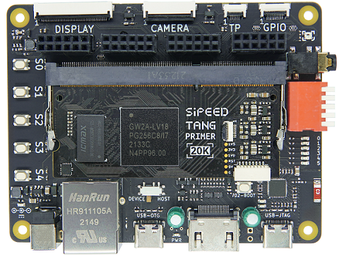
Let's take cheap small FPGA as a base.
AD9833 clean sine drive looks attractive. But one chip costs $12.
It could be replaced with direct digital synthesis inside FPGA with external DAC.
With DDS inside FPGA we know exact zero crossing position with subsample precision, and may avoid detecting it using drive signal feedback.
But fast 8-10bit DACs cost as AD9833 or even more expensive, and with smaller stock (issues with purchase in future may be expected).
Can we get DDS sine drive for (almost) free?
What if we replace expensive DAC with simple R2R ladder + opamp buffer?
R2R matrix costs $1-$2. What should be R resistance? What is max sample rate for R2R+cap+opamp based DAC?
Current sensing approach requires comparator which senses current through drive resistor.
Comparator cost is about $5-$7 (e.g. adcmp601).
Can we get current sensing comparator for free?
FPGA pins which support differential input have built-in comparator.
What if we can use it to sense current through drive resistor? Not sure about common mode range supported by this comparator.
If not possible, ok, let's use external comparator.
Gowin GW1N series 1K chips are in stock on Mouser for $7 / 1 pcs.
Some bigger chips provide interesting additional features. E.g. embedded RAM.
Example: GW1NR-LV4QN88C6/I5 is in stock on Mouser and about $19 / 1 pcs.
It has 8MB SDR SDRAM with 16bit data width - enough for reverb/delay, and for LCD framebuffer.
QFN88 is a bit hard to solder, but I think it is possible to order PCB assembly on JLCPCB.
If FPGA is cheap we can use separate chip per sensor to minimize mutual influence, and place sensors closer to antennas.
But probably, it's ok to use single FPGA for both sensors.
R2R DAC may be connected to different I/O banks, powered from separate LDO regulators.
It makes sense to make FPGA to DAC traces short, so connectors for both inductors will be close each other.
Does it make sense to use some shielded RF connection (SMA + coaxial cable) to connect both inductors with minimal interference between pitch and volume oscillators?
How to interface FPGA sensor with MCU?
MCU should be able to fetch sensor data with minimal CPU consumption. In ideal case, one measure per audio sample should be provided to MCU.
I2S looks like ideal for this. 48KHz, 24 bits per sample, stereo. 4 pins - MCLK, BCLK, LRCK, DATA.
24bit L/R samples will transferred from FPGA to MCU via I2S will hold values for pitch and volume - e.g. linearized hand position, or even pitch frequency + volume gain.
MCU will be able to receive I2S data using DMA, with handling of received data in audio IRQ - once per audio frame.
For controlling of FPGA part (e.g. setting calibration parameters, linearization parameters, etc) or reading some data we can use SPI interface.
How to program FPGA?
Option 1: JTAG connector for FPGA.
Option 2: programming via SPI slave - bitstream will be loaded into FPGA by MCU on startup.
Audio output.
Some audio codec chip (e.g. SGTL5000) may be used for Line In, Line Out, HP Out.
MCU will output sound via I2S interface.
With big FPGA, audio stream may be passed through FPGA for post-processing, e.g. applying some filters, effects (like reverb).
FPGA as well may mirror audio stream to S/PDIF output.
LCD and GUI.
Big FPGA may hold framebuffer, and MCU may draw UI via SPI using commands like fill rectangle, draw text, etc.


