Let's Design and Build a (mostly) Digital Theremin!

Posted: 9/29/2024 3:05:04 PM
dewster

From: Northern NJ, USA

Joined: 2/17/2012

"1) Is there a wiring plan to parts that are meant to be mounted in the housing and connected to main board connector J10 (or other connectors)? Or maybe even a breakout board that accomodates all the external connectors? Very likely there is no common scheme as different people have various housings and different needs for external connectors."  - gerbold

The J10 expansion port use is sort of on a case by case basis.  I wire up a ribbon cable to plug into it, and then solder the other ends to whatever connectors and switches are mounted on the I/O panel.  Here's a video of one version: https://www.youtube.com/watch?v=9Cs0PlpKx68

"2) Are the builtin Toslink and the serial interface all that is required to get started? The serial lines Rx and Tx are used to connect the command line librarian to d-lev, right?"

Yes.

"3) All mounting holes have a diameter of 3.2mm for M3. Just the mounting hole H5 of the d-lev_8mm_tuner has a diameter of 2.5 mm. Is the 2.5mm hole intended for cutting an M3 thread?"

Yes, tapping that hole works well.

"4) All 0.1µF ceramic C have 2.5mm pin distance. Not so C2 of the main baord which has 5mm. Does this C have to be electrically different compared to the others?"

You have a very sharp eye!  I would suggest you make C2 4.7uF (polarized tantalum as is used on the AFE boards - watch the polarity!) so that the LCD backlight operates in linear rather than switched mode.  This fixed an issue with internal interference that one user experienced.

"5) There are many one pin connectors of the type Con_01x01_Male. I assume the majority of these does not need to be assambled. Probabyl these are kind of test points or for future use.  d-lev_main: J12 (GND), J13 (+5V), J14 (+3.3V), J20 (gpio_i[2]), J21 (gpio_i[3]), J22 (gpio_o[2]), J23 (gpio_i[3]), J24 (mido_tx_o); mido_tx_o may be the inverted midi_tx_n_o; d-lev_tuner_driver: J3 (DP); d-lev_afe: J4 (GND), TP7 (C_DIV)."

Yes, no need to populate those.  [EDIT] Though TP7 (C_DIV) might come in handy for checking the divider voltage swing with a scope.

These two are probably required to connect the solenoid. But how exactly are the connections between antenna, solenoid, and d-lev_afe?  d-lev_afe: J2 (L_IN), J3 (L_OUT)"

The one labeled "Drive" connects to the "cold" or low impedance end of the solenoid.  The one labeled "Sense" connects to the "hot" or high impedance end of the solenoid and the antenna.

"Not clear about the ESD pin. The ESD plane is connected to the mounting solder pins of the EC11. As the mucisian touches these buttons, there is the risk of electrostatic discharge. What is to be done with these three pins?  d-lev_encoders: J8 (GND), J9 (ESD), J10 (GND)"

[EDIT] I just jumper the ESD hole to the GND hole.  To minimize ESD at the encoders I recommend all plastic knobs (I 3D print them) without set screws.

"6) The LCD type is not well specified..."

I agree, though probably any one you pick that genuinely takes 3.3V (i.e. has a charge pump IC) should work.  5V parts will work too, but like you say they would need jumpers.  I don't have direct experience here, but Evan Khan does.  The backlight is always powered via 5V to keep the load off the FPGA regulators, and this is done in a constant-current type way.

You will want to snip the contrast pot connection going to 3.3V though, that needs updating on the schematic.

"7) What are the properties of the power supply? 5V but how much A? Would a USB charger be good enough or does one need a low noise power supply? Recommendations?"

Any decent quality USB charger should do.  It needs 5V at somewhere around 0.5A.

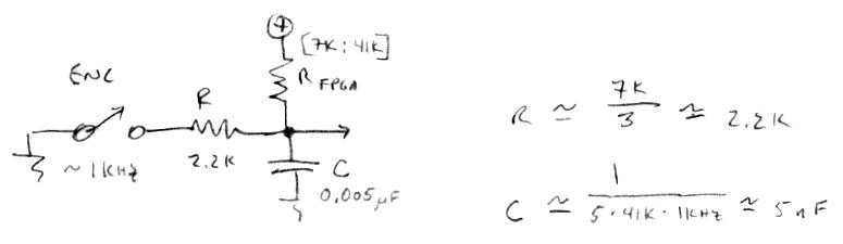
"8) The closest I can get to 38.1mm is PVC pipe with 40mm. Assuming 1mH and 2mH, these commands should calculate the solenoid, right?"

That should do it.  The values don't have to be spot-on, though purchasing an LC meter never hurts in this biz.

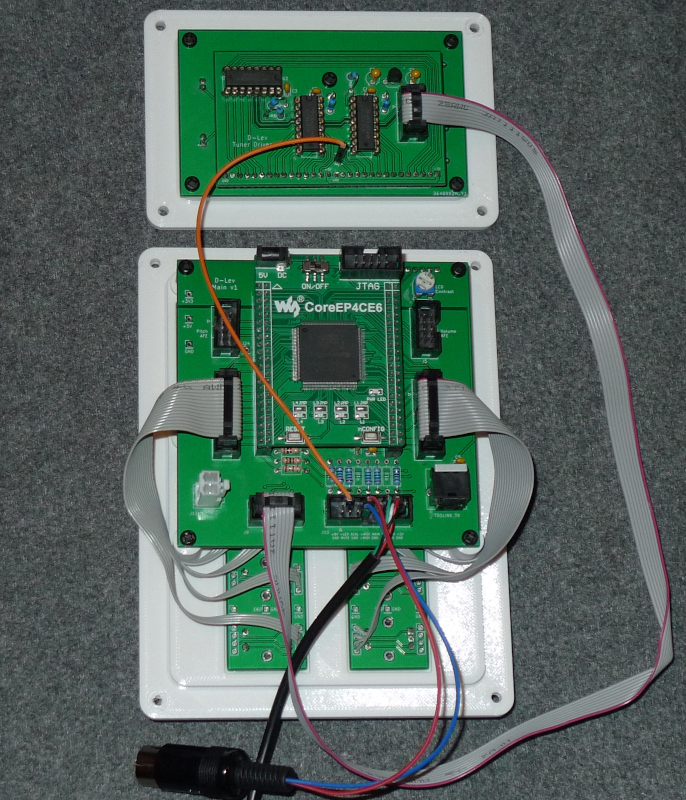
"9) It would be quite helpfull to have some pictures:"

I'll see what I can do, but all of the built-up boards I have here are already mounted to their 3D printed panels and boxes and such.  There isn't really all that much going on with the support circuitry, it's fairly non-critical, though there are things to watch out for when mounting the coils and AFE boards.

Posted: 9/30/2024 1:39:31 PM
gerbold

Joined: 9/26/2024

I'd like to add a debouncing the EC11 encoder switches. The topic has been discussed before: [1676][2814][3036][3037].
 is discussed in [1676]
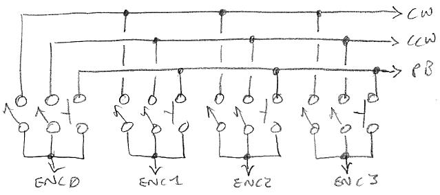
 [3036] refers to a circuit proposed by Bourns for PEC11R series
The disadvantage here is that it cannot be implemented in the encoder board without changing the signals of the connectors. There is no positive supply voltage at the moment.


The above would be an alternative. The image can be found several times in the internet with an image search, unfortunatelly it is not clear who the original author is. It is essentially the same as discussed in [1676] with the difference, that [1676] also shows the FPGA internal pullup.


This is again the same as [1676], annotated with some min/typ/max values from the Cyclone IV Device Datasheet. I've chosen 1k and 10nF as these values are already used in the D-Lev and calculated with a python script rise and fall times when opening or closing the switch for min/typ/max scenarios. The typical rise time is 0.17 ms, the typical fall time is 0.39 µs. This is in the range proposed by [2814] "... a detent cycle takes roughly 4ms, let's say 2ms worst case.  I would set the rise time to somewhere around 1/10 this, or 0.2ms."

Code:
R(max)   =2101, v_divider={'min': 0.1528186120971671, 'typ': 0.25583188812220947, 'max': 0.7999082518404571}
R(chosen)=1000, v_divider={'min': 0.07464285714285715, 'typ': 0.12692307692307692, 'max': 0.433125}
C(chosen)=10.0nF
rise times when opening the switch
pull_up= 7.0k, r=1.0k, vccio[min]=3.13V, v_c(start)[min]=0.39V, v_c(high)=1.71V, time=0.05ms
pull_up= 7.0k, r=1.0k, vccio[typ]=3.30V, v_c(start)[typ]=0.41V, v_c(high)=1.72V, time=0.04ms
pull_up= 7.0k, r=1.0k, vccio[max]=3.46V, v_c(start)[max]=0.43V, v_c(high)=1.70V, time=0.04ms
pull_up=25.0k, r=1.0k, vccio[min]=3.13V, v_c(start)[min]=0.12V, v_c(high)=1.70V, time=0.19ms
pull_up=25.0k, r=1.0k, vccio[typ]=3.30V, v_c(start)[typ]=0.13V, v_c(high)=1.71V, time=0.17ms
pull_up=25.0k, r=1.0k, vccio[max]=3.46V, v_c(start)[max]=0.13V, v_c(high)=1.70V, time=0.16ms
pull_up=41.0k, r=1.0k, vccio[min]=3.13V, v_c(start)[min]=0.07V, v_c(high)=1.70V, time=0.31ms
pull_up=41.0k, r=1.0k, vccio[typ]=3.30V, v_c(start)[typ]=0.08V, v_c(high)=1.70V, time=0.29ms
pull_up=41.0k, r=1.0k, vccio[max]=3.46V, v_c(start)[max]=0.08V, v_c(high)=1.70V, time=0.27ms
fall times when closing the switch
pull_up= 7.0k, r=1.0k, vccio[min]=3.13V, v_c(start)[min]=3.13V, v_c(low)=0.80V, time=0.13ms
pull_up= 7.0k, r=1.0k, vccio[typ]=3.30V, v_c(start)[typ]=3.30V, v_c(low)=0.80V, time=0.14ms
pull_up= 7.0k, r=1.0k, vccio[max]=3.46V, v_c(start)[max]=3.46V, v_c(low)=0.80V, time=0.15ms
pull_up=25.0k, r=1.0k, vccio[min]=3.13V, v_c(start)[min]=3.13V, v_c(low)=0.80V, time=0.37ms
pull_up=25.0k, r=1.0k, vccio[typ]=3.30V, v_c(start)[typ]=3.30V, v_c(low)=0.80V, time=0.39ms
pull_up=25.0k, r=1.0k, vccio[max]=3.46V, v_c(start)[max]=3.46V, v_c(low)=0.80V, time=0.40ms
pull_up=41.0k, r=1.0k, vccio[min]=3.13V, v_c(start)[min]=3.13V, v_c(low)=0.80V, time=0.59ms
pull_up=41.0k, r=1.0k, vccio[typ]=3.30V, v_c(start)[typ]=3.30V, v_c(low)=0.80V, time=0.61ms
pull_up=41.0k, r=1.0k, vccio[max]=3.46V, v_c(start)[max]=3.46V, v_c(low)=0.80V, time=0.64ms

With these results I modified the encoder schematics.

At this point starts my problem: I'd like to update the PCB. I open the PCB editor, press F8 and it generates 20 error messages, one for each of the newly added C and R. Originally I copied these from the main schematic. The error message says that it cannot find the footprints for "d-lev_footprints:R_Axial_DIN0207_L6.3mm_D2.5mm_P10.16mm_Horizontal" and "d-lev_footprints:C_Disc_D3.0mm_W2.0mm_P2.50mm". I'm sure these are present in the d-lev_footprints.pretty folder, but I fail to import them. My KiCad version is 8.05 release build. Any hint?

Posted: 9/30/2024 1:56:57 PM
dewster

From: Northern NJ, USA

Joined: 2/17/2012

"I'd like to add a debouncing the EC11 encoder switches."  - gerbold

I do understand the concern here.  But I would advise against it as it tends to really interfere with the velocity sensing.  The digital debouncing logic within the FPGA seems entirely adequate.  Another reason to avoid analog debouncing is future designs may (or may not!) implement the "DC Scanning" technique I proposed a while back to dramatically reduce encoder interconnect [LINK] (the second one without the transistors).  I believe debouncing is more to slow things down for capture by SW and interrupts and the like.

Not trying to discourage you or saying I did everything absolutely right, but there may be some value in building the kit "as is" at least for your first spin, as there can be a lot to take in, at least initially, and you will likely have your hands full as it is.

My broad advice here is to try not to "shoot it into the can" as movie types would put it.  Make things with an eye towards the generic rather than the specific, so you don't find yourself painted into a corner.  Early assumptions and decisions can tie your hands later.  Try to put off thinking about portability, compactness, beauty, etc. until the very end.  Ergonomics should reign supreme when designing a musical instrument.

Posted: 9/30/2024 2:14:59 PM
gerbold

Joined: 9/26/2024

Most likely found and fixed the issue: Hardcoded linux paths are used in the project files. This fails in Windows.

Code:
C:\Projects\Theremin\D-Lev\Open Source Design Files\d-lev_kicad_2023-07-25>grep -r d-lev_footprints.pretty
d-lev_8mm_tuner/fp-lib-table:  (lib (name "d-lev_footprints")(type "KiCad")(uri "/home/demo/Documents/KiCad/D-Lev/v2/d-lev_footprints.pretty")(options "")(descr ""))
d-lev_afe/fp-lib-table:  (lib (name "d-lev_footprints")(type "KiCad")(uri "/home/demo/Documents/KiCad/D-Lev/v2/d-lev_footprints.pretty")(options "")(descr ""))
d-lev_encoders/fp-lib-table:  (lib (name "d-lev_footprints")(type "KiCad")(uri "/home/demo/Documents/KiCad/D-Lev/v2/d-lev_footprints.pretty")(options "")(descr ""))
d-lev_main/fp-lib-table:  (lib (name "d-lev_footprints")(type "KiCad")(uri "/home/demo/Documents/KiCad/D-Lev/v2/d-lev_footprints.pretty")(options "")(descr ""))
d-lev_tuner_driver/fp-lib-table:  (lib (name "d-lev_footprints")(type "KiCad")(uri "/home/demo/Documents/KiCad/D-Lev/v2/d-lev_footprints.pretty")(options "")(descr ""))

Solution: The absolute path has to be replaced with a relative path in all these files. This should work for both: Linux and Windows.

old:

Code:
(uri "/home/demo/Documents/KiCad/D-Lev/v2/d-lev_footprints.pretty")

new:

Code:
(uri "../d-lev_footprints.pretty")


d-lev_8mm_tuner\fp-lib-table has another similar problem with 

Code:
uri "/home/demo/Documents/KiCad/Libraries/SparkFun-KiCad-Libraries-master/Footprints/LED.pretty".

LED.pretty is not even shared in the open source files.

Posted: 9/30/2024 2:18:11 PM
gerbold

Joined: 9/26/2024

"I do understand the concern here.  But I would advise against it as it tends to really interfere with the velocity sensing. .." - dewster
ok

Posted: 9/30/2024 2:42:14 PM
dewster

From: Northern NJ, USA

Joined: 2/17/2012

"Most likely found and fixed the issue: Hardcoded linux paths are used in the project files. This fails in Windows."  - gerbold

Thanks for that info!  I'm not a KiCad expert at all...

Posted: 10/1/2024 5:51:02 AM
gerbold

Joined: 9/26/2024

I'm a newbe in KiCad. Windows says I insatlled it September 26th.


The scheme to handle the rotatory switches in the linked post will require changes in both the main board and the encoder boards. There is no backward compatibility between the future scheme and the current encoder boards. The common pins that have to be fed back to the transistors (ENC[0..3]) is currently grounded. Thus there is no real reason to not modify todays encoder boards.

The change I proposed is for todays scheme. The changes are fully backward compatible as they can be rolled back to the orignal functionality.
- The 1k resistors won't probably be noticed by the FPGA anyway with todays scheme, but if the FPGA has issues with them I can replace them with 0 Ohm bridges and will be back to the original function.
- The 10nF capacitors if not assembled will not provide debouncing and thus again be back at the original function.

"But I would advise against it as it tends to really interfere with the velocity sensing." - dewster

I understand and will not assemble the Cs unless I see heavy bouncing that disturbs the function. In this case I'll tyr to get it fixed with HW debouncing. The changes are more like an optional safetybelt in case the switches I selected are poor regarding their bouncing behaviour. In this case I could try to get it fixed by assembling the capacitors.
Depending on the placeability of all the parts on a PCB with the same form factor I may drop the changes.

Posted: 10/2/2024 12:40:51 PM
dewster

From: Northern NJ, USA

Joined: 2/17/2012

"The scheme to handle the rotatory switches in the linked post will require changes in both the main board and the encoder boards. There is no backward compatibility between the future scheme and the current encoder boards. The common pins that have to be fed back to the transistors (ENC[0..3]) is currently grounded. Thus there is no real reason to not modify todays encoder boards."  - gerbold

True.  I imagine that I'm anticipating the possibility of a move to this, and analog debouncing would definitely interfere with it.  I'm thinking ENC[0:3] could perhaps be driven directly by open drain FPGA pins, rather than via transistors.

"- The 1k resistors won't probably be noticed by the FPGA anyway with todays scheme, but if the FPGA has issues with them I can replace them with 0 Ohm bridges and will be back to the original function.

- The 10nF capacitors if not assembled will not provide debouncing and thus again be back at the original function."

I suppose it never hurts to have some sort of backup plan when it comes to PCBs.  I guess I'm trying to keep you from worrying about small things that may appear disturbingly non-standard but aren't broken and work fine.  My feeling is that if the encoders are so flaky that they need analog debouncing to function, then they are likely 90% dead at that point anyway and need to be replaced.  If I were to change the current design here it might be to add optional external pullups to those now provided by the FPGA internally.

I think a lot of folks have had bad experiences with encoders in products, which isn't surprising given the presence of lame encoders out there and often poor HW / SW around them.  I've had better luck with the cheap E-Bay ones than the more expensive pedigreed ones from "reputable" dealers.

I would gently caution you against deviating too far from the kit with your initial build, particularly if you don't have a lot of experience with coils and Theremin fields.  If nothing else, it can provide a valuable baseline from which to proceed.  And the more your design differs from mine, the more difficult it may be for me to offer useful guidance.

Posted: 10/2/2024 6:50:47 PM
gerbold

Joined: 9/26/2024

Thanks for your reply, dewster.

I tried to understand how the mechanical asembly is done and identified a mechanical colission between the resistors and Cs I added and the LCD.

 step 1: encoders
 step 2: LCD
 step 3: main board

This leads to the next question: Are the left and right encoder board assembled in the same way or is the pcb for the right side flipped and assembled form the other side?

I tried to find a photo showing this. The closest I could get is this. But it shows an older version of the encoder board, I guess.

Posted: 10/2/2024 8:44:19 PM
dewster

From: Northern NJ, USA

Joined: 2/17/2012

"I tried to understand how the mechanical asembly is done and identified a mechanical colission between the resistors and Cs I added and the LCD."  - gerbold

Yes, that interference is very real.  I have to snip the top-most encoder mount tab flush after soldering it.  I cover it with a piece of insulating tape to keep it from shorting out to the LCD.

"Are the left and right encoder board assembled in the same way or is the pcb for the right side flipped and assembled form the other side?"

They're both assembled the same way, though I make the ribbon cable for one a bit longer to compensate for the extra distance to the mounting point.

[EDIT] Some more recent pix (taken today):


1. Above: Back view of controller unit.


2. Above: Bottom view.  Note ESD jumpers to GND, hot glue strain relief on encoder cables, blue tape insulation between encoders & LCD.  "Low profile" encoders wouldn't need this and the encoder PWBs would be flush with the 3D printed top surface.


3. Above: side view.  Note hot glue on ribbon cable.

You must be logged in to post a reply. Please log in or register for a new account.